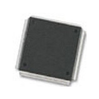
MC68376BAMFT20 Freescale Semiconductor, MC68376BAMFT20 Datasheet - Page 84

MC68376BAMFT20
Manufacturer Part Number
MC68376BAMFT20
Description
Manufacturer
Freescale Semiconductor
Datasheet
1.MC68376BAMFT20.pdf
(434 pages)
Specifications of MC68376BAMFT20
Cpu Family
68K/M683xx
Device Core
ColdFire
Device Core Size
32b
Frequency (max)
20MHz
Interface Type
QSPI/SCI
Program Memory Type
ROM
Program Memory Size
8KB
Total Internal Ram Size
7.5KB
# I/os (max)
18
Number Of Timers - General Purpose
2
Operating Supply Voltage (typ)
5V
Operating Supply Voltage (max)
5.25V
Operating Supply Voltage (min)
4.75V
On-chip Adc
16-chx10-bit
Instruction Set Architecture
RISC
Operating Temp Range
-40C to 125C
Operating Temperature Classification
Automotive
Mounting
Surface Mount
Pin Count
160
Package Type
PQFP
Lead Free Status / Rohs Status
Not Compliant
Available stocks
Company
Part Number
Manufacturer
Quantity
Price
Company:
Part Number:
MC68376BAMFT20
Manufacturer:
FREESCAL
Quantity:
245
- Current page: 84 of 434
- Download datasheet (7Mb)
5-6
MOTOROLA
1. MAINTAIN LOW LEAKAGE ON THE XFC NODE. REFER TO APPENDIX A ELECTRICAL CHARACTERISTICS FOR MORE INFORMATION.
2. RECOMMENDED LOOP FILTER FOR REDUCED SENSITIVITY TO LOW FREQUENCY NOISE.
A voltage controlled oscillator (VCO) in the PLL generates the system clock signal. To
maintain a 50% clock duty cycle, the VCO frequency (f
the system clock frequency, depending on the state of the X bit in SYNCR. The clock
signal is fed back to a divider/counter. The divider controls the frequency of one input
to a phase comparator. The other phase comparator input is a reference signal, either
from the crystal oscillator or from an external source. The comparator generates a con-
trol signal proportional to the difference in phase between the two inputs. This signal
is low-pass filtered and used to correct the VCO output frequency.
Filter circuit implementation can vary, depending upon the external environment and
required clock stability. Figure 5-4 shows two recommended system clock filter
networks. XFC pin leakage must be kept as low as possible to maintain optimum sta-
bility and PLL performance.
An external filter network connected to the XFC pin is not required when an external
system clock signal is applied and the PLL is disabled (MODCLK = 0 at reset). The
XFC pin must be left floating in this case.
The synthesizer locks when the VCO frequency is equal to f
by the filter time constant and by the amount of difference between the two comparator
inputs. Whenever a comparator input changes, the synthesizer must relock. Lock sta-
tus is shown by the SLOCK bit in SYNCR. During power-up, the MCU does not come
out of reset until the synthesizer locks. Crystal type, characteristic frequency, and lay-
out of external oscillator circuitry affect lock time.
V
SS
NORMAL OPERATING ENVIRONMENT
C3
C4
0.01 F
0.1 F
Figure 5-4 System Clock Filter Networks
C1
0.1 F
SYSTEM INTEGRATION MODULE
XFC
V
DDSYN
1
V
SS
HIGH-STABILITY OPERATING ENVIRONMENT
C3
C4
0.01 F
0.1 F
VCO
) is either two or four times
ref
. Lock time is affected
C1
0.1 F
C2
0.01 F
USER’S MANUAL
NORMAL/HIGH-STABILITY XFC CONN
R1
18 k
MC68336/376
XFC
V
DDSYN
1, 2
Related parts for MC68376BAMFT20
Image
Part Number
Description
Manufacturer
Datasheet
Request
R
Part Number:
Description:
Manufacturer:
Freescale Semiconductor, Inc
Datasheet:
Part Number:
Description:
Manufacturer:
Freescale Semiconductor, Inc
Datasheet:
Part Number:
Description:
Manufacturer:
Freescale Semiconductor, Inc
Datasheet:
Part Number:
Description:
Manufacturer:
Freescale Semiconductor, Inc
Datasheet:
Part Number:
Description:
Manufacturer:
Freescale Semiconductor, Inc
Datasheet:
Part Number:
Description:
Manufacturer:
Freescale Semiconductor, Inc
Datasheet:
Part Number:
Description:
Manufacturer:
Freescale Semiconductor, Inc
Datasheet:
Part Number:
Description:
Manufacturer:
Freescale Semiconductor, Inc
Datasheet:
Part Number:
Description:
Manufacturer:
Freescale Semiconductor, Inc
Datasheet:
Part Number:
Description:
Manufacturer:
Freescale Semiconductor, Inc
Datasheet:
Part Number:
Description:
Manufacturer:
Freescale Semiconductor, Inc
Datasheet:
Part Number:
Description:
Manufacturer:
Freescale Semiconductor, Inc
Datasheet:
Part Number:
Description:
Manufacturer:
Freescale Semiconductor, Inc
Datasheet:
Part Number:
Description:
Manufacturer:
Freescale Semiconductor, Inc
Datasheet:
Part Number:
Description:
Manufacturer:
Freescale Semiconductor, Inc
Datasheet:


