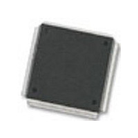
MC68376BAMFT20 Freescale Semiconductor, MC68376BAMFT20 Datasheet - Page 378

MC68376BAMFT20
Manufacturer Part Number
MC68376BAMFT20
Description
Manufacturer
Freescale Semiconductor
Datasheet
1.MC68376BAMFT20.pdf
(434 pages)
Specifications of MC68376BAMFT20
Cpu Family
68K/M683xx
Device Core
ColdFire
Device Core Size
32b
Frequency (max)
20MHz
Interface Type
QSPI/SCI
Program Memory Type
ROM
Program Memory Size
8KB
Total Internal Ram Size
7.5KB
# I/os (max)
18
Number Of Timers - General Purpose
2
Operating Supply Voltage (typ)
5V
Operating Supply Voltage (max)
5.25V
Operating Supply Voltage (min)
4.75V
On-chip Adc
16-chx10-bit
Instruction Set Architecture
RISC
Operating Temp Range
-40C to 125C
Operating Temperature Classification
Automotive
Mounting
Surface Mount
Pin Count
160
Package Type
PQFP
Lead Free Status / Rohs Status
Not Compliant
Available stocks
Company
Part Number
Manufacturer
Quantity
Price
Company:
Part Number:
MC68376BAMFT20
Manufacturer:
FREESCAL
Quantity:
245
- Current page: 378 of 434
- Download datasheet (7Mb)
IL[2:0] — Interrupt Level
IARB3 — Interrupt Arbitration Bit 3
DRV[A:B] — Drive Time Base Bus
IN — Clock Input Pin Status
CLK[2:0] — Counter Clock Select Field
D-60
MOTOROLA
When the FCSM generates an interrupt request, IL[2:0] determines which of the
interrupt request signals is asserted. When a request is acknowledged, the CTM4
compares IL[2:0] to a mask value supplied by the CPU32 to determine whether to
respond. IL[2:0] must have a value in the range of $0 (interrupts disabled) to $7
(highest priority).
This bit and the IARB[2:0] field in BIUMCR are concatenated to determine the interrupt
arbitration number for the submodule requesting interrupt service. Refer to D.7.1 BIU
Module Configuration Register for more information on IARB[2:0].
This field controls the connection of the FCSM to time base buses A and B. Refer to
Table D-39.
This read-only bit reflects the logic state of the clock input pin CTM2C. Writing to this
bit has no effect nor does reset.
These read/write control bits select one of the six CPSM clock signals (PCLK[1:6]) or
one of two external conditions on CTM2C to clock the free-running counter. The max-
imum frequency of an external clock signal is f
CLK2
0
0
0
0
1
1
1
1
Two time base buses should not be driven at the same time.
DRVA
0
0
1
1
CLK1
Table D-40 Counter Clock Select Field
Table D-39 Drive Time Base Bus Field
0
0
1
1
0
0
1
1
DRVB
0
1
0
1
CLK0
REGISTER SUMMARY
0
1
0
1
0
1
0
1
Neither time base bus A nor bus B is driven
Both time base bus A and bus B are driven
Prescaler output 6 (/64 or /512 or /96 to /768)
WARNING
Time base bus B is driven
Time base bus A is driven
Free Running Counter Clock Source
CTM2C input pin, negative edge
CTM2C input pin, positive edge
Prescaler output 4 (/16 or /24)
Prescaler output 5 (/32 or /48)
Prescaler output 3 (/8 or /12)
Prescaler output 1 (/2 or /3)
Prescaler output 2 (/4 or /6)
Bus Selected
sys
/4. Refer to Table D-40.
USER’S MANUAL
MC68336/376
Related parts for MC68376BAMFT20
Image
Part Number
Description
Manufacturer
Datasheet
Request
R
Part Number:
Description:
Manufacturer:
Freescale Semiconductor, Inc
Datasheet:
Part Number:
Description:
Manufacturer:
Freescale Semiconductor, Inc
Datasheet:
Part Number:
Description:
Manufacturer:
Freescale Semiconductor, Inc
Datasheet:
Part Number:
Description:
Manufacturer:
Freescale Semiconductor, Inc
Datasheet:
Part Number:
Description:
Manufacturer:
Freescale Semiconductor, Inc
Datasheet:
Part Number:
Description:
Manufacturer:
Freescale Semiconductor, Inc
Datasheet:
Part Number:
Description:
Manufacturer:
Freescale Semiconductor, Inc
Datasheet:
Part Number:
Description:
Manufacturer:
Freescale Semiconductor, Inc
Datasheet:
Part Number:
Description:
Manufacturer:
Freescale Semiconductor, Inc
Datasheet:
Part Number:
Description:
Manufacturer:
Freescale Semiconductor, Inc
Datasheet:
Part Number:
Description:
Manufacturer:
Freescale Semiconductor, Inc
Datasheet:
Part Number:
Description:
Manufacturer:
Freescale Semiconductor, Inc
Datasheet:
Part Number:
Description:
Manufacturer:
Freescale Semiconductor, Inc
Datasheet:
Part Number:
Description:
Manufacturer:
Freescale Semiconductor, Inc
Datasheet:
Part Number:
Description:
Manufacturer:
Freescale Semiconductor, Inc
Datasheet:


