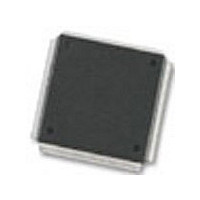
MC68376BAMFT20 Freescale Semiconductor, MC68376BAMFT20 Datasheet - Page 366

MC68376BAMFT20
Manufacturer Part Number
MC68376BAMFT20
Description
Manufacturer
Freescale Semiconductor
Datasheet
1.MC68376BAMFT20.pdf
(434 pages)
Specifications of MC68376BAMFT20
Cpu Family
68K/M683xx
Device Core
ColdFire
Device Core Size
32b
Frequency (max)
20MHz
Interface Type
QSPI/SCI
Program Memory Type
ROM
Program Memory Size
8KB
Total Internal Ram Size
7.5KB
# I/os (max)
18
Number Of Timers - General Purpose
2
Operating Supply Voltage (typ)
5V
Operating Supply Voltage (max)
5.25V
Operating Supply Voltage (min)
4.75V
On-chip Adc
16-chx10-bit
Instruction Set Architecture
RISC
Operating Temp Range
-40C to 125C
Operating Temperature Classification
Automotive
Mounting
Surface Mount
Pin Count
160
Package Type
PQFP
Lead Free Status / Rohs Status
Not Compliant
Available stocks
Company
Part Number
Manufacturer
Quantity
Price
Company:
Part Number:
MC68376BAMFT20
Manufacturer:
FREESCAL
Quantity:
245
- Current page: 366 of 434
- Download datasheet (7Mb)
D.6.11 QSPI Control Register 0
SPCR0 — QSPI Control Register 0
MSTR — Master/Slave Mode Select
WOMQ — Wired-OR Mode for QSPI Pins
D-48
MOTOROLA
RESET:
MSTR
15
0
DDRQS determines the direction of the TXD pin only when the SCI transmitter is dis-
abled. When the SCI transmitter is enabled, the TXD pin is an output.
SPCR0 contains parameters for configuring the QSPI and enabling various modes of
operation. The CPU32 has read/write access to SPCR0, but the QSM has read access
only. SPCR0 must be initialized before QSPI operation begins. Writing a new value to
SPCR0 while the QSPI is enabled disrupts operation.
0 = QSPI is a slave device.
1 = QSPI is the system master.
0 = Pins designated for output by DDRQS operate in normal mode.
1 = Pins designated for output by DDRQS operate in open-drain mode.
WOMQ
14
0
NOTES:
PCS0/SS
QSM Pin
PCS[1:3]
MISO
MOSI
SCK
TXD
1. PQS2 is a digital I/O pin unless the SPI is enabled (SPE set in SPCR1), in which case it
2. PQS7 is a digital I/O pin unless the SCI transmitter is enabled (TE set in SCCR1), in
RXD
becomes the QSPI serial clock SCK.
which case it becomes the SCI serial data output TXD.
13
0
1
2
Table D-33 Effect of DDRQS on QSM Pin Function
12
0
BITS[3:0]
Master
Master
Master
Master
Master
Mode
Slave
Slave
Slave
Slave
Slave
—
—
11
0
10
0
DDRQS Bit
DDQS[4:6]
DDQS0
DDQS1
DDQS2
DDQS3
DDQS7
None
REGISTER SUMMARY
CPOL
9
0
CPHA
8
1
Bit State
NA
—
—
X
0
1
0
1
0
1
0
1
0
1
0
1
0
1
0
1
7
0
6
0
Serial data output from QSPI
Serial data output from QSPI
Assertion causes mode fault
Serial data output from SCI
Disables chip-select output
Disables slave select Input
Serial data input to QSPI
Serial data input to QSPI
Clock output from QSPI
QSPI slave select input
Serial data input to SCI
5
0
Disables data output
Disables data output
Clock input to QSPI
Disables data input
Disables data input
Chip-select output
Chip-select output
Pin Function
Inactive
Inactive
4
0
SPBR[7:0]
3
0
USER’S MANUAL
2
1
MC68336/376
$YFFC18
1
0
0
0
Related parts for MC68376BAMFT20
Image
Part Number
Description
Manufacturer
Datasheet
Request
R
Part Number:
Description:
Manufacturer:
Freescale Semiconductor, Inc
Datasheet:
Part Number:
Description:
Manufacturer:
Freescale Semiconductor, Inc
Datasheet:
Part Number:
Description:
Manufacturer:
Freescale Semiconductor, Inc
Datasheet:
Part Number:
Description:
Manufacturer:
Freescale Semiconductor, Inc
Datasheet:
Part Number:
Description:
Manufacturer:
Freescale Semiconductor, Inc
Datasheet:
Part Number:
Description:
Manufacturer:
Freescale Semiconductor, Inc
Datasheet:
Part Number:
Description:
Manufacturer:
Freescale Semiconductor, Inc
Datasheet:
Part Number:
Description:
Manufacturer:
Freescale Semiconductor, Inc
Datasheet:
Part Number:
Description:
Manufacturer:
Freescale Semiconductor, Inc
Datasheet:
Part Number:
Description:
Manufacturer:
Freescale Semiconductor, Inc
Datasheet:
Part Number:
Description:
Manufacturer:
Freescale Semiconductor, Inc
Datasheet:
Part Number:
Description:
Manufacturer:
Freescale Semiconductor, Inc
Datasheet:
Part Number:
Description:
Manufacturer:
Freescale Semiconductor, Inc
Datasheet:
Part Number:
Description:
Manufacturer:
Freescale Semiconductor, Inc
Datasheet:
Part Number:
Description:
Manufacturer:
Freescale Semiconductor, Inc
Datasheet:


