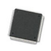
MC68376BAMFT20 Freescale Semiconductor, MC68376BAMFT20 Datasheet - Page 188

MC68376BAMFT20
Manufacturer Part Number
MC68376BAMFT20
Description
Manufacturer
Freescale Semiconductor
Datasheet
1.MC68376BAMFT20.pdf
(434 pages)
Specifications of MC68376BAMFT20
Cpu Family
68K/M683xx
Device Core
ColdFire
Device Core Size
32b
Frequency (max)
20MHz
Interface Type
QSPI/SCI
Program Memory Type
ROM
Program Memory Size
8KB
Total Internal Ram Size
7.5KB
# I/os (max)
18
Number Of Timers - General Purpose
2
Operating Supply Voltage (typ)
5V
Operating Supply Voltage (max)
5.25V
Operating Supply Voltage (min)
4.75V
On-chip Adc
16-chx10-bit
Instruction Set Architecture
RISC
Operating Temp Range
-40C to 125C
Operating Temperature Classification
Automotive
Mounting
Surface Mount
Pin Count
160
Package Type
PQFP
Lead Free Status / Rohs Status
Not Compliant
Available stocks
Company
Part Number
Manufacturer
Quantity
Price
Company:
Part Number:
MC68376BAMFT20
Manufacturer:
FREESCAL
Quantity:
245
- Current page: 188 of 434
- Download datasheet (7Mb)
8.4.7 Dedicated Analog Supply Pins
8.4.8 External Digital Supply Pin
8.4.9 Digital Supply Pins
8.5 QADC Bus Interface
8.6 Module Configuration
8.6.1 Low-Power Stop Mode
8-6
MOTOROLA
V
Dedicated power is required to isolate the sensitive analog circuitry from the normal
levels of noise present on the digital power supply. Refer to Tables A-11 and A-12 for
more information.
Each port A pin includes a digital open drain output driver, an analog input signal path,
and a digital input synchronizer. The V
on the port A pins. Since the QADC output pins have open drain type drivers, a dedi-
cated V
V
digital MCU modules.
The QADC can respond to byte, word, and long word accesses, however, coherency
is not provided for accesses that require more than one bus cycle.
For example, if a long word read of two consecutive result registers is initiated, the
QADC could change one of the result registers between the bus cycles required for
each register read. All read and write accesses that require more than one 16-bit
access to complete occur as two or more independent bus cycles.
Normal reads from and writes to the QADC require two clock cycles. However, if the
CPU32 tries to access locations that are also accessible to the QADC while the QADC
is accessing them, the bus cycle will require additional clock cycles. The QADC may
insert from one to four wait states in the process of a CPU32 read from or write to such
a location.
The QADC module configuration register (QADCMCR) defines freeze and stop mode
operation, supervisor space access, and interrupt arbitration priority. Unimplemented
bits read zero and writes have no effect. QADCMCR is typically written once when
software initializes the QADC, and not changed thereafter. Refer to D.5.1 QADC Mod-
ule Configuration Register for register and bit descriptions.
When the STOP bit in QADCMCR is set, the clock signal to the A/D converter is dis-
abled, effectively turning off the analog circuitry. This results in a static, low power con-
sumption, idle condition. Low-power stop mode aborts any conversion sequence in
progress. Because the bias currents to the analog circuits are turned off in low-power
stop mode, the QADC requires some recovery time (t
CAL CHARACTERISTICS) to stabilize the analog circuits after the STOP bit is
cleared.
DDA
DD
and V
and V
DD
SS
pin is not needed.
SSA
provide the power for the digital portions of the QADC, and for all other
QUEUED ANALOG-TO-DIGITAL CONVERTER MODULE
pins supply power to the analog subsystems of the QADC module.
SS
pin provides the ground level for the drivers
SR
in APPENDIX A ELECTRI-
USER’S MANUAL
MC68336/376
Related parts for MC68376BAMFT20
Image
Part Number
Description
Manufacturer
Datasheet
Request
R
Part Number:
Description:
Manufacturer:
Freescale Semiconductor, Inc
Datasheet:
Part Number:
Description:
Manufacturer:
Freescale Semiconductor, Inc
Datasheet:
Part Number:
Description:
Manufacturer:
Freescale Semiconductor, Inc
Datasheet:
Part Number:
Description:
Manufacturer:
Freescale Semiconductor, Inc
Datasheet:
Part Number:
Description:
Manufacturer:
Freescale Semiconductor, Inc
Datasheet:
Part Number:
Description:
Manufacturer:
Freescale Semiconductor, Inc
Datasheet:
Part Number:
Description:
Manufacturer:
Freescale Semiconductor, Inc
Datasheet:
Part Number:
Description:
Manufacturer:
Freescale Semiconductor, Inc
Datasheet:
Part Number:
Description:
Manufacturer:
Freescale Semiconductor, Inc
Datasheet:
Part Number:
Description:
Manufacturer:
Freescale Semiconductor, Inc
Datasheet:
Part Number:
Description:
Manufacturer:
Freescale Semiconductor, Inc
Datasheet:
Part Number:
Description:
Manufacturer:
Freescale Semiconductor, Inc
Datasheet:
Part Number:
Description:
Manufacturer:
Freescale Semiconductor, Inc
Datasheet:
Part Number:
Description:
Manufacturer:
Freescale Semiconductor, Inc
Datasheet:
Part Number:
Description:
Manufacturer:
Freescale Semiconductor, Inc
Datasheet:


