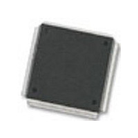
MC68376BAMFT20 Freescale Semiconductor, MC68376BAMFT20 Datasheet - Page 247

MC68376BAMFT20
Manufacturer Part Number
MC68376BAMFT20
Description
Manufacturer
Freescale Semiconductor
Datasheet
1.MC68376BAMFT20.pdf
(434 pages)
Specifications of MC68376BAMFT20
Cpu Family
68K/M683xx
Device Core
ColdFire
Device Core Size
32b
Frequency (max)
20MHz
Interface Type
QSPI/SCI
Program Memory Type
ROM
Program Memory Size
8KB
Total Internal Ram Size
7.5KB
# I/os (max)
18
Number Of Timers - General Purpose
2
Operating Supply Voltage (typ)
5V
Operating Supply Voltage (max)
5.25V
Operating Supply Voltage (min)
4.75V
On-chip Adc
16-chx10-bit
Instruction Set Architecture
RISC
Operating Temp Range
-40C to 125C
Operating Temperature Classification
Automotive
Mounting
Surface Mount
Pin Count
160
Package Type
PQFP
Lead Free Status / Rohs Status
Not Compliant
Available stocks
Company
Part Number
Manufacturer
Quantity
Price
Company:
Part Number:
MC68376BAMFT20
Manufacturer:
FREESCAL
Quantity:
245
- Current page: 247 of 434
- Download datasheet (7Mb)
11.5.9 Frequency Measurement (FQM)
11.5.10 Hall Effect Decode (HALLD)
11.6 Host Interface Registers
11.6.1 System Configuration Registers
11.6.1.1 Prescaler Control for TCR1
MC68336/376
USER’S MANUAL
FQM counts the number of input pulses to a TPU channel during a user-defined win-
dow period. The function has single shot and continuous modes. No pulses are lost
between sample windows in continuous mode. The user selects whether to detect
pulses on the rising or falling edge. This function is intended for high speed measure-
ment; measurement of slow pulses with noise rejection can be made with PTA.
Refer to TPU programming note Frequency Measurement (FQM) TPU Function
(TPUPN03/D) for more information.
This function decodes the sensor signals from a brushless motor, along with a direc-
tion input from the CPU32, into a state number. The function supports two- or three-
sensor decoding. The decoded state number is written into a COMM channel, which
outputs the required commutation drive signals. In addition to brushless motor appli-
cations, the function can have more general applications, such as decoding option
switches.
Refer to TPU programming note Hall Effect Decode (HALLD) TPU Function
(TPUPN10/D) for more information.
The TPU memory map contains three groups of registers:
All registers except the channel interrupt status register (CISR) must be read or written
by means of word accesses. The address space of the TPU memory map occupies
512 bytes. Unused registers within the 512-byte address space return zeros when
read.
The TPU configuration control registers, TPUMCR and TICR, determine the value of
the prescaler, perform emulation control, specify whether the external TCR2 pin func-
tions as a clock source or as gate of the DIV8 clock for TCR2, and determine interrupt
request level and interrupt vector number assignment. Refer to D.8.1 TPU Module
Configuration Register and D.8.5 TPU Interrupt Configuration Register for more
information about TPUMCR and TICR.
Timer count register one (TCR1) is clocked from the output of a prescaler. Two fields
in TPUMCR control TCR1. The prescaler's input is the internal TPU system clock
divided by either 4 or 32, depending on the value of the PSCK bit. The prescaler
divides this input by 1, 2, 4, or 8, depending on the value of TCR1P. Channels using
• System configuration registers
• Channel control and status registers
• Development support and test verification registers
TIME PROCESSOR UNIT
MOTOROLA
11-13
Related parts for MC68376BAMFT20
Image
Part Number
Description
Manufacturer
Datasheet
Request
R
Part Number:
Description:
Manufacturer:
Freescale Semiconductor, Inc
Datasheet:
Part Number:
Description:
Manufacturer:
Freescale Semiconductor, Inc
Datasheet:
Part Number:
Description:
Manufacturer:
Freescale Semiconductor, Inc
Datasheet:
Part Number:
Description:
Manufacturer:
Freescale Semiconductor, Inc
Datasheet:
Part Number:
Description:
Manufacturer:
Freescale Semiconductor, Inc
Datasheet:
Part Number:
Description:
Manufacturer:
Freescale Semiconductor, Inc
Datasheet:
Part Number:
Description:
Manufacturer:
Freescale Semiconductor, Inc
Datasheet:
Part Number:
Description:
Manufacturer:
Freescale Semiconductor, Inc
Datasheet:
Part Number:
Description:
Manufacturer:
Freescale Semiconductor, Inc
Datasheet:
Part Number:
Description:
Manufacturer:
Freescale Semiconductor, Inc
Datasheet:
Part Number:
Description:
Manufacturer:
Freescale Semiconductor, Inc
Datasheet:
Part Number:
Description:
Manufacturer:
Freescale Semiconductor, Inc
Datasheet:
Part Number:
Description:
Manufacturer:
Freescale Semiconductor, Inc
Datasheet:
Part Number:
Description:
Manufacturer:
Freescale Semiconductor, Inc
Datasheet:
Part Number:
Description:
Manufacturer:
Freescale Semiconductor, Inc
Datasheet:


