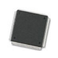
MC68376BAMFT20 Freescale Semiconductor, MC68376BAMFT20 Datasheet - Page 213

MC68376BAMFT20
Manufacturer Part Number
MC68376BAMFT20
Description
Manufacturer
Freescale Semiconductor
Datasheet
1.MC68376BAMFT20.pdf
(434 pages)
Specifications of MC68376BAMFT20
Cpu Family
68K/M683xx
Device Core
ColdFire
Device Core Size
32b
Frequency (max)
20MHz
Interface Type
QSPI/SCI
Program Memory Type
ROM
Program Memory Size
8KB
Total Internal Ram Size
7.5KB
# I/os (max)
18
Number Of Timers - General Purpose
2
Operating Supply Voltage (typ)
5V
Operating Supply Voltage (max)
5.25V
Operating Supply Voltage (min)
4.75V
On-chip Adc
16-chx10-bit
Instruction Set Architecture
RISC
Operating Temp Range
-40C to 125C
Operating Temperature Classification
Automotive
Mounting
Surface Mount
Pin Count
160
Package Type
PQFP
Lead Free Status / Rohs Status
Not Compliant
Available stocks
Company
Part Number
Manufacturer
Quantity
Price
Company:
Part Number:
MC68376BAMFT20
Manufacturer:
FREESCAL
Quantity:
245
- Current page: 213 of 434
- Download datasheet (7Mb)
8.12.8 Result Word Table
MC68336/376
USER’S MANUAL
When any of the end-of-queue conditions is recognized, a queue completion flag is
set, and if enabled, an interrupt request is generated. The following situations prema-
turely terminate queue execution:
The result word table is a 40-word long, 10-bit wide RAM. The QADC writes a result
word after completing an analog conversion specified by the corresponding CCW. The
result word table can be read or written, but in normal operation, software reads the
result word table to obtain analog conversions from the QADC. Unimplemented bits
are read as zeros, and write operations have no effect. Refer to D.5.9 Result Word
Table for register descriptions.
While there is only one result word table, the data can be accessed in three different
alignment formats:
The left justified, signed format corresponds to a half-scale, offset binary, two’s com-
plement data format. The data is routed onto the IMB according to the selected format.
The address used to access the table determines the data alignment format. All write
operations to the result word table are right justified.
• Since queue 1 is higher in priority than queue 2, when a trigger event occurs on
• When a queue is disabled, any conversion taking place for that queue is aborted.
• When the operating mode of a queue is changed to another valid mode, any
• When placed in low-power stop mode, the QADC aborts any conversion in
• When the FRZ bit in the QADCMCR is set and the IMB FREEZE line is asserted,
1. Right justified, with zeros in the higher order unused bits.
2. Left justified, with the most significant bit inverted to form a sign bit, and zeros
3. Left justified, with zeros in the unused lower order bits.
queue 1 during queue 2 execution, the execution of queue 2 is suspended by
aborting execution of the CCW in progress, and queue 1 execution begins. When
queue 1 execution is complete, queue 2 conversions restart with the first CCW
entry in queue 2 or the first CCW of the queue 2 subqueue being executed when
queue 2 was suspended. Alternately, conversions can restart with the aborted
queue 2 CCW entry. The resume RES bit in QACR2 allows software to select
where queue 2 begins after suspension. By choosing to re-execute all of the sus-
pended queue 2 and subqueue CCWs, all of the samples are guaranteed to have
been taken during the same scan pass. However, a high trigger event rate for
queue 1 can prohibit the completion of queue 2. If this occurs, execution of queue
2 may begin with the aborted CCW entry.
Putting a queue into disabled mode does not power down the converter.
conversion taking place for that queue is aborted. The queue operating restarts
at the beginning of the queue, once an appropriate trigger event occurs.
progress.
the QADC freezes at the end of the current conversion. When FREEZE is negat-
ed, the QADC resumes queue execution beginning with the next CCW entry.
in the unused lower order bits.
QUEUED ANALOG-TO-DIGITAL CONVERTER MODULE
MOTOROLA
8-31
Related parts for MC68376BAMFT20
Image
Part Number
Description
Manufacturer
Datasheet
Request
R
Part Number:
Description:
Manufacturer:
Freescale Semiconductor, Inc
Datasheet:
Part Number:
Description:
Manufacturer:
Freescale Semiconductor, Inc
Datasheet:
Part Number:
Description:
Manufacturer:
Freescale Semiconductor, Inc
Datasheet:
Part Number:
Description:
Manufacturer:
Freescale Semiconductor, Inc
Datasheet:
Part Number:
Description:
Manufacturer:
Freescale Semiconductor, Inc
Datasheet:
Part Number:
Description:
Manufacturer:
Freescale Semiconductor, Inc
Datasheet:
Part Number:
Description:
Manufacturer:
Freescale Semiconductor, Inc
Datasheet:
Part Number:
Description:
Manufacturer:
Freescale Semiconductor, Inc
Datasheet:
Part Number:
Description:
Manufacturer:
Freescale Semiconductor, Inc
Datasheet:
Part Number:
Description:
Manufacturer:
Freescale Semiconductor, Inc
Datasheet:
Part Number:
Description:
Manufacturer:
Freescale Semiconductor, Inc
Datasheet:
Part Number:
Description:
Manufacturer:
Freescale Semiconductor, Inc
Datasheet:
Part Number:
Description:
Manufacturer:
Freescale Semiconductor, Inc
Datasheet:
Part Number:
Description:
Manufacturer:
Freescale Semiconductor, Inc
Datasheet:
Part Number:
Description:
Manufacturer:
Freescale Semiconductor, Inc
Datasheet:


