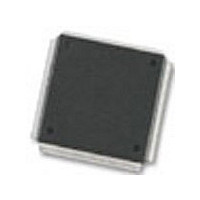
MC68376BAMFT20 Freescale Semiconductor, MC68376BAMFT20 Datasheet - Page 76

MC68376BAMFT20
Manufacturer Part Number
MC68376BAMFT20
Description
Manufacturer
Freescale Semiconductor
Datasheet
1.MC68376BAMFT20.pdf
(434 pages)
Specifications of MC68376BAMFT20
Cpu Family
68K/M683xx
Device Core
ColdFire
Device Core Size
32b
Frequency (max)
20MHz
Interface Type
QSPI/SCI
Program Memory Type
ROM
Program Memory Size
8KB
Total Internal Ram Size
7.5KB
# I/os (max)
18
Number Of Timers - General Purpose
2
Operating Supply Voltage (typ)
5V
Operating Supply Voltage (max)
5.25V
Operating Supply Voltage (min)
4.75V
On-chip Adc
16-chx10-bit
Instruction Set Architecture
RISC
Operating Temp Range
-40C to 125C
Operating Temperature Classification
Automotive
Mounting
Surface Mount
Pin Count
160
Package Type
PQFP
Lead Free Status / Rohs Status
Not Compliant
Available stocks
Company
Part Number
Manufacturer
Quantity
Price
Company:
Part Number:
MC68376BAMFT20
Manufacturer:
FREESCAL
Quantity:
245
- Current page: 76 of 434
- Download datasheet (7Mb)
4-24
MOTOROLA
MICROSEQUENCER
The serial interface uses a full-duplex synchronous protocol similar to the serial pe-
ripheral interface (SPI) protocol. The development system serves as the master of the
serial link since it is responsible for the generation of DSCLK. If DSCLK is derived from
the CPU32 system clock, development system serial logic is unhindered by the oper-
ating frequency of the target processor. Operable frequency range of the serial clock
is from DC to one-half the processor system clock frequency.
The serial interface operates in full-duplex mode — data is transmitted and received
simultaneously by both master and slave devices. In general, data transitions occur on
the falling edge of DSCLK and are stable by the following rising edge of DSCLK. Data
is transmitted MSB first, and is latched on the rising edge of DSCLK.
The serial data word is 17 bits wide, including 16 data bits and a status/control bit (refer
to Figure 4-11). Bit 16 indicates the status of CPU-generated messages. Table 4-7
shows the CPU-generated message types.
CPU
SYNCHRONIZE
EXECUTION
STATUS
UNIT
Figure 4-10 Debug Serial I/O Block Diagram
PARALLEL OUT
RCV DATA LATCH
REGISTER BUS
PARALLEL IN
INSTRUCTION
SERIAL OUT
SERIAL IN
CENTRAL PROCESSOR UNIT
16
16
CONTROL
LOGIC
M
DSCLK
DSO
DSI
DEVELOPMENT SYSTEM
STATUS
0
COMMAND LATCH
PARALLEL OUT
RESULT LATCH
CONTROL
PARALLEL IN
SERIAL OUT
LOGIC
SERIAL IN
DATA
DATA
16
16
USER’S MANUAL
MC68336/376
SERIAL
32 DEBUG I/O BLOCK
CLOCK
Related parts for MC68376BAMFT20
Image
Part Number
Description
Manufacturer
Datasheet
Request
R
Part Number:
Description:
Manufacturer:
Freescale Semiconductor, Inc
Datasheet:
Part Number:
Description:
Manufacturer:
Freescale Semiconductor, Inc
Datasheet:
Part Number:
Description:
Manufacturer:
Freescale Semiconductor, Inc
Datasheet:
Part Number:
Description:
Manufacturer:
Freescale Semiconductor, Inc
Datasheet:
Part Number:
Description:
Manufacturer:
Freescale Semiconductor, Inc
Datasheet:
Part Number:
Description:
Manufacturer:
Freescale Semiconductor, Inc
Datasheet:
Part Number:
Description:
Manufacturer:
Freescale Semiconductor, Inc
Datasheet:
Part Number:
Description:
Manufacturer:
Freescale Semiconductor, Inc
Datasheet:
Part Number:
Description:
Manufacturer:
Freescale Semiconductor, Inc
Datasheet:
Part Number:
Description:
Manufacturer:
Freescale Semiconductor, Inc
Datasheet:
Part Number:
Description:
Manufacturer:
Freescale Semiconductor, Inc
Datasheet:
Part Number:
Description:
Manufacturer:
Freescale Semiconductor, Inc
Datasheet:
Part Number:
Description:
Manufacturer:
Freescale Semiconductor, Inc
Datasheet:
Part Number:
Description:
Manufacturer:
Freescale Semiconductor, Inc
Datasheet:
Part Number:
Description:
Manufacturer:
Freescale Semiconductor, Inc
Datasheet:


