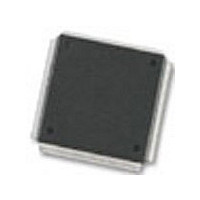
MC68376BAMFT20 Freescale Semiconductor, MC68376BAMFT20 Datasheet - Page 368

MC68376BAMFT20
Manufacturer Part Number
MC68376BAMFT20
Description
Manufacturer
Freescale Semiconductor
Datasheet
1.MC68376BAMFT20.pdf
(434 pages)
Specifications of MC68376BAMFT20
Cpu Family
68K/M683xx
Device Core
ColdFire
Device Core Size
32b
Frequency (max)
20MHz
Interface Type
QSPI/SCI
Program Memory Type
ROM
Program Memory Size
8KB
Total Internal Ram Size
7.5KB
# I/os (max)
18
Number Of Timers - General Purpose
2
Operating Supply Voltage (typ)
5V
Operating Supply Voltage (max)
5.25V
Operating Supply Voltage (min)
4.75V
On-chip Adc
16-chx10-bit
Instruction Set Architecture
RISC
Operating Temp Range
-40C to 125C
Operating Temperature Classification
Automotive
Mounting
Surface Mount
Pin Count
160
Package Type
PQFP
Lead Free Status / Rohs Status
Not Compliant
Available stocks
Company
Part Number
Manufacturer
Quantity
Price
Company:
Part Number:
MC68376BAMFT20
Manufacturer:
FREESCAL
Quantity:
245
- Current page: 368 of 434
- Download datasheet (7Mb)
D.6.12 QSPI Control Register 1
SPCR1 — QSPI Control Register 1
SPE — QSPI Enable
DSCKL[6:0] — Delay before SCK
D-50
MOTOROLA
RESET:
SPE
15
0
Giving SPBR[7:0] a value of zero or one disables the baud rate generator. SCK is
disabled and assumes its inactive state value. No serial transfers occur. At reset, the
SCK baud rate is initialized to one eighth of the system clock frequency.
SPCR1 enables the QSPI and specified transfer delays. The CPU32 has read/write
access to SPCR1, but the QSM has read access only to all bits except SPE. SPCR1
must be written last during initialization because it contains SPE. Writing a new value
to SPCR1 while the QSPI is enabled disrupts operation.
When the DSCK bit is set in a command RAM byte, this field determines the length of
the delay from PCS valid to SCK transition. PCS can be any of the four peripheral chip-
select pins. The following equation determines the actual delay before SCK:
where DSCKL[6:0] equals is in the range of 1 to 127.
When DSCK is zero in a command RAM byte, then DSCKL[6:0] is not used. Instead,
the PCS valid to SCK transition is one-half the SCK period.
0 = QSPI is disabled. QSPI pins can be used for general-purpose I/O.
1 = QSPI is enabled. Pins allocated by PQSPAR are controlled by the QSPI.
14
0
13
0
12
0
DSCKL[6:0]
11
0
SPBR[7:0]
PCS to SCK Delay
SCK Baud Rate
10
1
REGISTER SUMMARY
9
0
=
------------------------------------------------------------------------- -
2 SCK Baud Rate Desired
8
0
or
7
0
=
------------------------------------ -
2 SPBR[7:0]
=
6
0
DSCKL[6:0]
------------------------------ -
f
sys
f
sys
f
sys
5
0
4
0
DTL[7:0]
3
0
USER’S MANUAL
2
1
MC68336/376
$YFFC1A
1
0
0
0
Related parts for MC68376BAMFT20
Image
Part Number
Description
Manufacturer
Datasheet
Request
R
Part Number:
Description:
Manufacturer:
Freescale Semiconductor, Inc
Datasheet:
Part Number:
Description:
Manufacturer:
Freescale Semiconductor, Inc
Datasheet:
Part Number:
Description:
Manufacturer:
Freescale Semiconductor, Inc
Datasheet:
Part Number:
Description:
Manufacturer:
Freescale Semiconductor, Inc
Datasheet:
Part Number:
Description:
Manufacturer:
Freescale Semiconductor, Inc
Datasheet:
Part Number:
Description:
Manufacturer:
Freescale Semiconductor, Inc
Datasheet:
Part Number:
Description:
Manufacturer:
Freescale Semiconductor, Inc
Datasheet:
Part Number:
Description:
Manufacturer:
Freescale Semiconductor, Inc
Datasheet:
Part Number:
Description:
Manufacturer:
Freescale Semiconductor, Inc
Datasheet:
Part Number:
Description:
Manufacturer:
Freescale Semiconductor, Inc
Datasheet:
Part Number:
Description:
Manufacturer:
Freescale Semiconductor, Inc
Datasheet:
Part Number:
Description:
Manufacturer:
Freescale Semiconductor, Inc
Datasheet:
Part Number:
Description:
Manufacturer:
Freescale Semiconductor, Inc
Datasheet:
Part Number:
Description:
Manufacturer:
Freescale Semiconductor, Inc
Datasheet:
Part Number:
Description:
Manufacturer:
Freescale Semiconductor, Inc
Datasheet:


