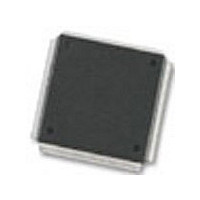
MC68376BAMFT20 Freescale Semiconductor, MC68376BAMFT20 Datasheet - Page 197

MC68376BAMFT20
Manufacturer Part Number
MC68376BAMFT20
Description
Manufacturer
Freescale Semiconductor
Datasheet
1.MC68376BAMFT20.pdf
(434 pages)
Specifications of MC68376BAMFT20
Cpu Family
68K/M683xx
Device Core
ColdFire
Device Core Size
32b
Frequency (max)
20MHz
Interface Type
QSPI/SCI
Program Memory Type
ROM
Program Memory Size
8KB
Total Internal Ram Size
7.5KB
# I/os (max)
18
Number Of Timers - General Purpose
2
Operating Supply Voltage (typ)
5V
Operating Supply Voltage (max)
5.25V
Operating Supply Voltage (min)
4.75V
On-chip Adc
16-chx10-bit
Instruction Set Architecture
RISC
Operating Temp Range
-40C to 125C
Operating Temperature Classification
Automotive
Mounting
Surface Mount
Pin Count
160
Package Type
PQFP
Lead Free Status / Rohs Status
Not Compliant
Available stocks
Company
Part Number
Manufacturer
Quantity
Price
Company:
Part Number:
MC68376BAMFT20
Manufacturer:
FREESCAL
Quantity:
245
- Current page: 197 of 434
- Download datasheet (7Mb)
8.11.2 Front-End Analog Multiplexer
8.11.3 Digital to Analog Converter Array
MC68336/376
USER’S MANUAL
The internal multiplexer selects one of the 16 analog input pins or one of three special
internal reference channels for conversion. The following are the three special chan-
nels:
The selected input is connected to one side of the DAC capacitor array. The other side
of the DAC array is connected to the comparator input. The multiplexer also includes
positive and negative stress protection circuitry, which prevents other channels from
affecting the current conversion when voltage levels are applied to the other channels.
Refer to APPENDIX A ELECTRICAL CHARACTERISTICS for specific voltage level
limits.
The digital to analog converter (DAC) array consists of binary-weighted capacitors and
a resistor-divider chain. The array serves two purposes:
Resolution begins with the MSB and works down to the LSB. The switching sequence
is controlled by the digital logic.
• V
• V
• V
• The array holds the sampled input voltage during conversion.
• The resistor-capacitor array provides the mechanism for the successive approx-
imation A/D conversion.
RH
RL
DDA
— Reference Voltage Low
— Reference Voltage High
QCLK
/2 — Mid-Analog Supply Voltage
QUEUED ANALOG-TO-DIGITAL CONVERTER MODULE
Figure 8-6 Bypass Mode Conversion Timing
N CYCLES:
(2, 4, 8, 16)
SAMPLE
SAMPLE
TIME
TIME
SUCCESSIVE APPROXIMATION RESOLUTION
RESOLUTION
SEQUENCE
10 CYCLES
TIME
QADC BYP CONVERSION TIM
MOTOROLA
8-15
Related parts for MC68376BAMFT20
Image
Part Number
Description
Manufacturer
Datasheet
Request
R
Part Number:
Description:
Manufacturer:
Freescale Semiconductor, Inc
Datasheet:
Part Number:
Description:
Manufacturer:
Freescale Semiconductor, Inc
Datasheet:
Part Number:
Description:
Manufacturer:
Freescale Semiconductor, Inc
Datasheet:
Part Number:
Description:
Manufacturer:
Freescale Semiconductor, Inc
Datasheet:
Part Number:
Description:
Manufacturer:
Freescale Semiconductor, Inc
Datasheet:
Part Number:
Description:
Manufacturer:
Freescale Semiconductor, Inc
Datasheet:
Part Number:
Description:
Manufacturer:
Freescale Semiconductor, Inc
Datasheet:
Part Number:
Description:
Manufacturer:
Freescale Semiconductor, Inc
Datasheet:
Part Number:
Description:
Manufacturer:
Freescale Semiconductor, Inc
Datasheet:
Part Number:
Description:
Manufacturer:
Freescale Semiconductor, Inc
Datasheet:
Part Number:
Description:
Manufacturer:
Freescale Semiconductor, Inc
Datasheet:
Part Number:
Description:
Manufacturer:
Freescale Semiconductor, Inc
Datasheet:
Part Number:
Description:
Manufacturer:
Freescale Semiconductor, Inc
Datasheet:
Part Number:
Description:
Manufacturer:
Freescale Semiconductor, Inc
Datasheet:
Part Number:
Description:
Manufacturer:
Freescale Semiconductor, Inc
Datasheet:


