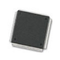
MC68376BAMFT20 Freescale Semiconductor, MC68376BAMFT20 Datasheet - Page 134

MC68376BAMFT20
Manufacturer Part Number
MC68376BAMFT20
Description
Manufacturer
Freescale Semiconductor
Datasheet
1.MC68376BAMFT20.pdf
(434 pages)
Specifications of MC68376BAMFT20
Cpu Family
68K/M683xx
Device Core
ColdFire
Device Core Size
32b
Frequency (max)
20MHz
Interface Type
QSPI/SCI
Program Memory Type
ROM
Program Memory Size
8KB
Total Internal Ram Size
7.5KB
# I/os (max)
18
Number Of Timers - General Purpose
2
Operating Supply Voltage (typ)
5V
Operating Supply Voltage (max)
5.25V
Operating Supply Voltage (min)
4.75V
On-chip Adc
16-chx10-bit
Instruction Set Architecture
RISC
Operating Temp Range
-40C to 125C
Operating Temperature Classification
Automotive
Mounting
Surface Mount
Pin Count
160
Package Type
PQFP
Lead Free Status / Rohs Status
Not Compliant
Available stocks
Company
Part Number
Manufacturer
Quantity
Price
Company:
Part Number:
MC68376BAMFT20
Manufacturer:
FREESCAL
Quantity:
245
- Current page: 134 of 434
- Download datasheet (7Mb)
5-56
MOTOROLA
Chip-select assertion can be synchronized with bus control signals to provide output
enable, read/write strobe, or interrupt acknowledge signals. Chip-select logic can also
generate DSACK and AVEC signals internally. A single DSACK generator is shared
by all chip-selects. Each signal can also be synchronized with the ECLK signal avail-
able on ADDR23.
When a memory access occurs, chip-select logic compares address space type, ad-
dress, type of access, transfer size, and interrupt priority (in the case of interrupt ac-
knowledge) to parameters stored in chip-select registers. If all parameters match, the
appropriate chip-select signal is asserted. Select signals are active low.
If a chip-select function is given the same address as a microcontroller module or an
internal memory array, an access to that address goes to the module or array, and the
chip-select signal is not asserted. The external address and data buses do not reflect
the internal access.
All chip-select circuits are configured for operation out of reset. However, all chip-se-
lect signals except CSBOOT are disabled, and cannot be asserted until the BYTE[1:0]
field in the corresponding option register is programmed to a non-zero value to select
a transfer size. The chip-select option register must not be written until a base address
has been written to a proper base address register. Alternate functions for chip-select
pins are enabled if appropriate data bus pins are held low at the release of RESET.
Refer to 5.7.3.1 Data Bus Mode Selection for more information. Figure 5-20 is a
functional diagram of a single chip-select circuit.
DSACK
BUS CONTROL
AVEC
ADDRESS
INTERNAL
SIGNALS
Figure 5-20 Chip-Select Circuit Block Diagram
GENERATOR
AVEC
BASE ADDRESS REGISTER
ADDRESS COMPARATOR
SYSTEM INTEGRATION MODULE
OPTION COMPARE
OPTION REGISTER
GENERATOR
DSACK
ASSIGNMENT
REGISTER
PIN
CONTROL
TIMING
AND
REGISTER
DATA
PIN
USER’S MANUAL
PIN
MC68336/376
CHIP SEL BLOCK
Related parts for MC68376BAMFT20
Image
Part Number
Description
Manufacturer
Datasheet
Request
R
Part Number:
Description:
Manufacturer:
Freescale Semiconductor, Inc
Datasheet:
Part Number:
Description:
Manufacturer:
Freescale Semiconductor, Inc
Datasheet:
Part Number:
Description:
Manufacturer:
Freescale Semiconductor, Inc
Datasheet:
Part Number:
Description:
Manufacturer:
Freescale Semiconductor, Inc
Datasheet:
Part Number:
Description:
Manufacturer:
Freescale Semiconductor, Inc
Datasheet:
Part Number:
Description:
Manufacturer:
Freescale Semiconductor, Inc
Datasheet:
Part Number:
Description:
Manufacturer:
Freescale Semiconductor, Inc
Datasheet:
Part Number:
Description:
Manufacturer:
Freescale Semiconductor, Inc
Datasheet:
Part Number:
Description:
Manufacturer:
Freescale Semiconductor, Inc
Datasheet:
Part Number:
Description:
Manufacturer:
Freescale Semiconductor, Inc
Datasheet:
Part Number:
Description:
Manufacturer:
Freescale Semiconductor, Inc
Datasheet:
Part Number:
Description:
Manufacturer:
Freescale Semiconductor, Inc
Datasheet:
Part Number:
Description:
Manufacturer:
Freescale Semiconductor, Inc
Datasheet:
Part Number:
Description:
Manufacturer:
Freescale Semiconductor, Inc
Datasheet:
Part Number:
Description:
Manufacturer:
Freescale Semiconductor, Inc
Datasheet:


