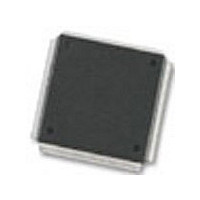
MC68376BAMFT20 Freescale Semiconductor, MC68376BAMFT20 Datasheet - Page 355

MC68376BAMFT20
Manufacturer Part Number
MC68376BAMFT20
Description
Manufacturer
Freescale Semiconductor
Datasheet
1.MC68376BAMFT20.pdf
(434 pages)
Specifications of MC68376BAMFT20
Cpu Family
68K/M683xx
Device Core
ColdFire
Device Core Size
32b
Frequency (max)
20MHz
Interface Type
QSPI/SCI
Program Memory Type
ROM
Program Memory Size
8KB
Total Internal Ram Size
7.5KB
# I/os (max)
18
Number Of Timers - General Purpose
2
Operating Supply Voltage (typ)
5V
Operating Supply Voltage (max)
5.25V
Operating Supply Voltage (min)
4.75V
On-chip Adc
16-chx10-bit
Instruction Set Architecture
RISC
Operating Temp Range
-40C to 125C
Operating Temperature Classification
Automotive
Mounting
Surface Mount
Pin Count
160
Package Type
PQFP
Lead Free Status / Rohs Status
Not Compliant
Available stocks
Company
Part Number
Manufacturer
Quantity
Price
Company:
Part Number:
MC68376BAMFT20
Manufacturer:
FREESCAL
Quantity:
245
- Current page: 355 of 434
- Download datasheet (7Mb)
CCW[0:27] — Conversion Command Word Table
D.5.8 Conversion Command Word Table
P — Pause
BYP — Sample Amplifier Bypass
IST[1:0] — Input Sample Time
CHAN[5:0] — Channel Number
MC68336/376
USER’S MANUAL
RESET:
15
The pause bit allows the creation of sub-queues within queue 1 and queue 2. The
QADC performs the conversion specified by the CCW with the pause bit set, and then
the queue enters the pause state. Another trigger event causes execution to continue
from the pause to the next CCW.
Setting BYP enables the amplifier bypass mode for a conversion, and subsequently
changes the timing. Refer to 8.11.1.1 Amplifier Bypass Mode Conversion Timing
for more information.
The IST field specifies the length of the sample window. Longer sample times permit
more accurate A/D conversions of signals with higher source impedances.
Table D-28 shows the bit encoding of the IST field.
The CHAN field selects the input channel number corresponding to the analog input
pin to be sampled and converted. The analog input pin channel number assignments
and the pin definitions vary depending on whether the QADC is operating in multi-
plexed or non-multiplexed mode. The queue scan mechanism sees no distinction be-
tween an internally or externally multiplexed analog input.
CHAN specifies a reserved channel number (channels 32 to 47) or an invalid channel
number (channels 4 to 31 in non-multiplexed mode), the low reference level (V
converted. Programming the channel field to channel 63 indicates the end of the
queue. Channels 60 to 62 are special internal channels. When one of these channels
is selected, the sample amplifier is not used. The value of V
placed directly onto the converter. Programming the input sample time to any value
other than two for one of the internal channels has no benefit except to lengthen the
overall conversion time.
0 = Do not enter the pause state after execution of the current CCW.
1 = Enter the pause state after execution of the current CCW.
0 = Amplifier bypass mode disabled.
1 = Amplifier bypass mode enabled.
14
13
NOT USED
12
IST[1:0]
11
00
01
10
11
Table D-28 Input Sample Times
10
REGISTER SUMMARY
U
9
P
BYP
U
8
Input Sample Times
16 QCLK periods
2 QCLK periods
4 QCLK periods
8 QCLK periods
U
7
IST[1:0]
6
U
U
5
U
4
RL
$YFF230–$YFF27E
, V
U
3
CHAN[5:0]
RH
U
, or V
2
MOTOROLA
U
1
DDA
RL
/2 is
D-37
U
) is
0
Related parts for MC68376BAMFT20
Image
Part Number
Description
Manufacturer
Datasheet
Request
R
Part Number:
Description:
Manufacturer:
Freescale Semiconductor, Inc
Datasheet:
Part Number:
Description:
Manufacturer:
Freescale Semiconductor, Inc
Datasheet:
Part Number:
Description:
Manufacturer:
Freescale Semiconductor, Inc
Datasheet:
Part Number:
Description:
Manufacturer:
Freescale Semiconductor, Inc
Datasheet:
Part Number:
Description:
Manufacturer:
Freescale Semiconductor, Inc
Datasheet:
Part Number:
Description:
Manufacturer:
Freescale Semiconductor, Inc
Datasheet:
Part Number:
Description:
Manufacturer:
Freescale Semiconductor, Inc
Datasheet:
Part Number:
Description:
Manufacturer:
Freescale Semiconductor, Inc
Datasheet:
Part Number:
Description:
Manufacturer:
Freescale Semiconductor, Inc
Datasheet:
Part Number:
Description:
Manufacturer:
Freescale Semiconductor, Inc
Datasheet:
Part Number:
Description:
Manufacturer:
Freescale Semiconductor, Inc
Datasheet:
Part Number:
Description:
Manufacturer:
Freescale Semiconductor, Inc
Datasheet:
Part Number:
Description:
Manufacturer:
Freescale Semiconductor, Inc
Datasheet:
Part Number:
Description:
Manufacturer:
Freescale Semiconductor, Inc
Datasheet:
Part Number:
Description:
Manufacturer:
Freescale Semiconductor, Inc
Datasheet:


