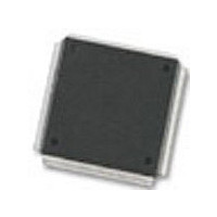
MC68376BAMFT20 Freescale Semiconductor, MC68376BAMFT20 Datasheet - Page 82

MC68376BAMFT20
Manufacturer Part Number
MC68376BAMFT20
Description
Manufacturer
Freescale Semiconductor
Datasheet
1.MC68376BAMFT20.pdf
(434 pages)
Specifications of MC68376BAMFT20
Cpu Family
68K/M683xx
Device Core
ColdFire
Device Core Size
32b
Frequency (max)
20MHz
Interface Type
QSPI/SCI
Program Memory Type
ROM
Program Memory Size
8KB
Total Internal Ram Size
7.5KB
# I/os (max)
18
Number Of Timers - General Purpose
2
Operating Supply Voltage (typ)
5V
Operating Supply Voltage (max)
5.25V
Operating Supply Voltage (min)
4.75V
On-chip Adc
16-chx10-bit
Instruction Set Architecture
RISC
Operating Temp Range
-40C to 125C
Operating Temperature Classification
Automotive
Mounting
Surface Mount
Pin Count
160
Package Type
PQFP
Lead Free Status / Rohs Status
Not Compliant
Available stocks
Company
Part Number
Manufacturer
Quantity
Price
Company:
Part Number:
MC68376BAMFT20
Manufacturer:
FREESCAL
Quantity:
245
- Current page: 82 of 434
- Download datasheet (7Mb)
5.3 System Clock
5.3.1 Clock Sources
5-4
MOTOROLA
MODCLK
The system clock in the SIM provides timing signals for the IMB modules and for an
external peripheral bus. Because the MCU is a fully static design, register and memory
contents are not affected when the clock rate changes. System hardware and software
support changes in clock rate during operation.
The system clock signal can be generated from one of two sources. An internal phase-
locked loop (PLL) can synthesize the clock from a fast reference, or the clock signal
can be directly input from an external frequency source. The fast reference is typically
a 4.194 MHz crystal, but may be generated by sources other than a crystal. Keep
these sources in mind while reading the rest of this section. Refer to Table A-4 in the
APPENDIX A ELECTRICAL CHARACTERISTICS for clock specifications.
Figure 5-2 is a block diagram of the clock submodule.
The state of the clock mode (MODCLK) pin during reset determines the system clock
source. When MODCLK is held high during reset, the clock synthesizer generates a
clock signal from an external reference frequency. The clock synthesizer control reg-
ister (SYNCR) determines operating frequency and mode of operation. When MOD-
CLK is held low during reset, the clock synthesizer is disabled and an external system
clock signal must be driven onto the EXTAL pin.
The input clock is referred to as f
source. The output of the clock system is referred to as f
are within normal operating limits.
EXTAL
OSCILLATOR
CRYSTAL
XTAL
Figure 5-2 System Clock Block Diagram
128
SYSTEM INTEGRATION MODULE
COMPARATOR
PHASE
ref
, and can be either a crystal or an external clock
SYSTEM CLOCK CONTROL
FEEDBACK DIVIDER
LOW-PASS
FILTER
XFC
sys
W
Y
X
. Ensure that f
V
VCO
DDSYN
USER’S MANUAL
SYSTEM
CLOCK
MC68336/376
ref
16/32 PLL BLOCK 4M
and f
CLKOUT
sys
Related parts for MC68376BAMFT20
Image
Part Number
Description
Manufacturer
Datasheet
Request
R
Part Number:
Description:
Manufacturer:
Freescale Semiconductor, Inc
Datasheet:
Part Number:
Description:
Manufacturer:
Freescale Semiconductor, Inc
Datasheet:
Part Number:
Description:
Manufacturer:
Freescale Semiconductor, Inc
Datasheet:
Part Number:
Description:
Manufacturer:
Freescale Semiconductor, Inc
Datasheet:
Part Number:
Description:
Manufacturer:
Freescale Semiconductor, Inc
Datasheet:
Part Number:
Description:
Manufacturer:
Freescale Semiconductor, Inc
Datasheet:
Part Number:
Description:
Manufacturer:
Freescale Semiconductor, Inc
Datasheet:
Part Number:
Description:
Manufacturer:
Freescale Semiconductor, Inc
Datasheet:
Part Number:
Description:
Manufacturer:
Freescale Semiconductor, Inc
Datasheet:
Part Number:
Description:
Manufacturer:
Freescale Semiconductor, Inc
Datasheet:
Part Number:
Description:
Manufacturer:
Freescale Semiconductor, Inc
Datasheet:
Part Number:
Description:
Manufacturer:
Freescale Semiconductor, Inc
Datasheet:
Part Number:
Description:
Manufacturer:
Freescale Semiconductor, Inc
Datasheet:
Part Number:
Description:
Manufacturer:
Freescale Semiconductor, Inc
Datasheet:
Part Number:
Description:
Manufacturer:
Freescale Semiconductor, Inc
Datasheet:


