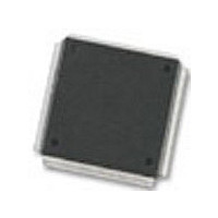
MC68376BAMFT20 Freescale Semiconductor, MC68376BAMFT20 Datasheet - Page 195

MC68376BAMFT20
Manufacturer Part Number
MC68376BAMFT20
Description
Manufacturer
Freescale Semiconductor
Datasheet
1.MC68376BAMFT20.pdf
(434 pages)
Specifications of MC68376BAMFT20
Cpu Family
68K/M683xx
Device Core
ColdFire
Device Core Size
32b
Frequency (max)
20MHz
Interface Type
QSPI/SCI
Program Memory Type
ROM
Program Memory Size
8KB
Total Internal Ram Size
7.5KB
# I/os (max)
18
Number Of Timers - General Purpose
2
Operating Supply Voltage (typ)
5V
Operating Supply Voltage (max)
5.25V
Operating Supply Voltage (min)
4.75V
On-chip Adc
16-chx10-bit
Instruction Set Architecture
RISC
Operating Temp Range
-40C to 125C
Operating Temperature Classification
Automotive
Mounting
Surface Mount
Pin Count
160
Package Type
PQFP
Lead Free Status / Rohs Status
Not Compliant
Available stocks
Company
Part Number
Manufacturer
Quantity
Price
Company:
Part Number:
MC68376BAMFT20
Manufacturer:
FREESCAL
Quantity:
245
- Current page: 195 of 434
- Download datasheet (7Mb)
8.11.1 Conversion Cycle Times
MC68336/376
USER’S MANUAL
VDDA
VSSA
PQA7
PQA0
PQB7
PQB0
VRH
VRL
Total conversion time is made up of initial sample time, transfer time, final sample time,
and resolution time. Initial sample time refers to the time during which the selected in-
put channel is connected to the sample capacitor at the input of the sample buffer am-
plifier. During the transfer period, the sample capacitor is disconnected from the
multiplexer, and the stored voltage is buffered and transferred to the RC DAC array.
During the final sampling period, the sample capacitor and amplifier are bypassed,
and the multiplexer input charges the RC DAC array directly. During the resolution pe-
riod, the voltage in the RC DAC array is converted to a digital value and stored in the
SAR.
Initial sample time is fixed at two QCLKs and the transfer time at four QCLKs. Final
sample time can be 2, 4, 8, or 16 ADC clock cycles, depending on the value of the IST
field in the CCW. Resolution time is ten cycles.
Transfer and resolution require a minimum of 18 QCLK clocks (8.6 s with a 2.1 MHz
QCLK). If the maximum final sample time period of 16 QCLKs is selected, the total
conversion time is 15.2 s with a 2.1 MHz QCLK.
CHARGE
PUMP
BIAS
AND
SAMPLE/
DUMMY
HOLD
DAC
CHAN. MUX
COMPAR-
QUEUED ANALOG-TO-DIGITAL CONVERTER MODULE
MUX 4: 1
ATOR
16: 2
Figure 8-4 QADC Module Block Diagram
SAMPLE/
HOLD
RC-DAC
10-BIT
APPROXIMATION
SUCCESSIVE
REGISTER
EXTERNAL
TRIGGERS
SAMPLE
TIMER
RESULT TABLE
CONTROL REGISTERS
CCW TABLE
AND CONTROL LOGIC
ADDRESS
40-WORD
40-WORD
DECODE
10-BIT,
10-BIT,
RAM
RAM
PERIODIC
TIMER
PORT PQA
I/O
PRESCALER
ALIGNMENT
RESULT
CLOCK
PORT PQB
INPUT
ADDRESS
DECODE
MOTOROLA
QADC DETAIL BLOCK
MODULE
CLOCK
INTER-
INTER-
DATA
ADDR
FACE
BUS
BUS
IMB
8-13
Related parts for MC68376BAMFT20
Image
Part Number
Description
Manufacturer
Datasheet
Request
R
Part Number:
Description:
Manufacturer:
Freescale Semiconductor, Inc
Datasheet:
Part Number:
Description:
Manufacturer:
Freescale Semiconductor, Inc
Datasheet:
Part Number:
Description:
Manufacturer:
Freescale Semiconductor, Inc
Datasheet:
Part Number:
Description:
Manufacturer:
Freescale Semiconductor, Inc
Datasheet:
Part Number:
Description:
Manufacturer:
Freescale Semiconductor, Inc
Datasheet:
Part Number:
Description:
Manufacturer:
Freescale Semiconductor, Inc
Datasheet:
Part Number:
Description:
Manufacturer:
Freescale Semiconductor, Inc
Datasheet:
Part Number:
Description:
Manufacturer:
Freescale Semiconductor, Inc
Datasheet:
Part Number:
Description:
Manufacturer:
Freescale Semiconductor, Inc
Datasheet:
Part Number:
Description:
Manufacturer:
Freescale Semiconductor, Inc
Datasheet:
Part Number:
Description:
Manufacturer:
Freescale Semiconductor, Inc
Datasheet:
Part Number:
Description:
Manufacturer:
Freescale Semiconductor, Inc
Datasheet:
Part Number:
Description:
Manufacturer:
Freescale Semiconductor, Inc
Datasheet:
Part Number:
Description:
Manufacturer:
Freescale Semiconductor, Inc
Datasheet:
Part Number:
Description:
Manufacturer:
Freescale Semiconductor, Inc
Datasheet:


