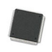
MC68376BAMFT20 Freescale Semiconductor, MC68376BAMFT20 Datasheet - Page 428

MC68376BAMFT20
Manufacturer Part Number
MC68376BAMFT20
Description
Manufacturer
Freescale Semiconductor
Datasheet
1.MC68376BAMFT20.pdf
(434 pages)
Specifications of MC68376BAMFT20
Cpu Family
68K/M683xx
Device Core
ColdFire
Device Core Size
32b
Frequency (max)
20MHz
Interface Type
QSPI/SCI
Program Memory Type
ROM
Program Memory Size
8KB
Total Internal Ram Size
7.5KB
# I/os (max)
18
Number Of Timers - General Purpose
2
Operating Supply Voltage (typ)
5V
Operating Supply Voltage (max)
5.25V
Operating Supply Voltage (min)
4.75V
On-chip Adc
16-chx10-bit
Instruction Set Architecture
RISC
Operating Temp Range
-40C to 125C
Operating Temperature Classification
Automotive
Mounting
Surface Mount
Pin Count
160
Package Type
PQFP
Lead Free Status / Rohs Status
Not Compliant
Available stocks
Company
Part Number
Manufacturer
Quantity
Price
Company:
Part Number:
MC68376BAMFT20
Manufacturer:
FREESCAL
Quantity:
245
- Current page: 428 of 434
- Download datasheet (7Mb)
Queue 1
Queue 2
Queued
R/W 5-22, 5-27
RAF D-45
RAM
RAMBAH 6-1, D-23
RAMBAL 6-1, D-23
RAMDS 12-1, D-83
RAMMCR 6-1, D-22
RAMTST 6-1, D-23
RASP 6-1, D-22, D-82
RDR 9-24
RDRF 9-28, D-45
RE 9-28, D-44
Read
Receive
MOTOROLA
I-12
status (QS) D-36
completion
interrupt level (IRLQ1) D-29
operating mode (MQ1) D-32
pause
single-scan enable (SSE1) D-32
trigger overrun (TOR1) D-35
completion
interrupt level (IRLQ2) D-29
operating mode (MQ2) D-33
pause
resume (RES) D-34
single-scan enable bit (SSE2) D-33
trigger overrun (TOR2) D-36
analog-to-digital converter. See QADC 8-1
output match (QOM) 11-11
serial
field 5-59, D-19
array
base address lock (RLCK) bit D-22
encoding D-22
/write signal (R/W) 5-22
cycle 5-28
system register command (RSREG) 4-20
end queue pointer (ENDQP) 9-8
new queue pointer (NEWQP) 9-8
flag (CF1) D-35
interrupt enable (CIE1) D-32
flag (PF1) D-35
interrupt enable (PIE1) D-32
flag (CF2) D-35
interrupt enable (CIE2) D-33
flag (PF2) D-35
interrupt enable (PIE2) D-33
module (QSM). See QSM 9-1
peripheral interface (QSPI) 9-1, 9-5
disable (RAMDS) D-83
space (RASP) D-22
flowchart 5-28
timing diagram A-11
–R–
Receiver
Reception of transmitted frames 13-13
Remote
RES 8-31, D-34
Reserved
RESET 4-19, 5-40, 5-42, 5-46, 5-47
Reset
Resistor-divider chain 8-15
Resolution time 8-13
Result word table 8-1, 8-16, 8-31
Resynchronization jump width (RJW) bit field D-91
Retry operation 5-37
RIE D-44
Right justified, unsigned result word table (RJURR) D-39
RJURR D-39
RJW 13-11, D-91
RLCK 6-1, D-22
RMC 3-7, 3-10, 3-12, 5-38
ROM array space (ASPC) D-25
ROMBAH 7-1, D-26
ROMBAL 7-1, D-26
ROMBS 7-1
ROMBS0-3 D-27
RPC 4-22
RR D-53
RS-232C terminal C-2
RSIGHI 7-1, 7-3, D-26
RSIGLO 7-1, 7-3, D-26
RSR 5-14, D-9
RSREG 4-20
RT 9-28
data
error status flag (RXWARN) D-95
pin configuration control (RXMODE) D-89
RAM 9-7
time sample clock (RT) 9-26, 9-28
active (RAF) D-45
data register (RDRF) flag 9-28
enable (RE) 9-28, D-44
interrupt enable (RIE) D-44
wakeup (RWU) 9-29, D-44
frames 13-15
transmission request (RTR) 13-4, 13-5
channel number D-37
mode 8-20
control logic in SIM 5-40
exception processing 5-40
mode selection
module pin function out of reset 5-45
operation in SIM 5-40
power-on 5-48
processing summary 5-50
source summary in SIM 5-41
states of pins assigned to other MCU modules 5-47
status register (RSR) 5-14, 5-50, D-9
timing 5-47
(RXD) pin 9-24
register full (RDRF) D-45
timing diagram A-18
use in determining SIM configuration 5-41
USER’S MANUAL
MC68336/376
Related parts for MC68376BAMFT20
Image
Part Number
Description
Manufacturer
Datasheet
Request
R
Part Number:
Description:
Manufacturer:
Freescale Semiconductor, Inc
Datasheet:
Part Number:
Description:
Manufacturer:
Freescale Semiconductor, Inc
Datasheet:
Part Number:
Description:
Manufacturer:
Freescale Semiconductor, Inc
Datasheet:
Part Number:
Description:
Manufacturer:
Freescale Semiconductor, Inc
Datasheet:
Part Number:
Description:
Manufacturer:
Freescale Semiconductor, Inc
Datasheet:
Part Number:
Description:
Manufacturer:
Freescale Semiconductor, Inc
Datasheet:
Part Number:
Description:
Manufacturer:
Freescale Semiconductor, Inc
Datasheet:
Part Number:
Description:
Manufacturer:
Freescale Semiconductor, Inc
Datasheet:
Part Number:
Description:
Manufacturer:
Freescale Semiconductor, Inc
Datasheet:
Part Number:
Description:
Manufacturer:
Freescale Semiconductor, Inc
Datasheet:
Part Number:
Description:
Manufacturer:
Freescale Semiconductor, Inc
Datasheet:
Part Number:
Description:
Manufacturer:
Freescale Semiconductor, Inc
Datasheet:
Part Number:
Description:
Manufacturer:
Freescale Semiconductor, Inc
Datasheet:
Part Number:
Description:
Manufacturer:
Freescale Semiconductor, Inc
Datasheet:
Part Number:
Description:
Manufacturer:
Freescale Semiconductor, Inc
Datasheet:


