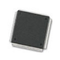
MC68376BAMFT20 Freescale Semiconductor, MC68376BAMFT20 Datasheet - Page 176

MC68376BAMFT20
Manufacturer Part Number
MC68376BAMFT20
Description
Manufacturer
Freescale Semiconductor
Datasheet
1.MC68376BAMFT20.pdf
(434 pages)
Specifications of MC68376BAMFT20
Cpu Family
68K/M683xx
Device Core
ColdFire
Device Core Size
32b
Frequency (max)
20MHz
Interface Type
QSPI/SCI
Program Memory Type
ROM
Program Memory Size
8KB
Total Internal Ram Size
7.5KB
# I/os (max)
18
Number Of Timers - General Purpose
2
Operating Supply Voltage (typ)
5V
Operating Supply Voltage (max)
5.25V
Operating Supply Voltage (min)
4.75V
On-chip Adc
16-chx10-bit
Instruction Set Architecture
RISC
Operating Temp Range
-40C to 125C
Operating Temperature Classification
Automotive
Mounting
Surface Mount
Pin Count
160
Package Type
PQFP
Lead Free Status / Rohs Status
Not Compliant
Available stocks
Company
Part Number
Manufacturer
Quantity
Price
Company:
Part Number:
MC68376BAMFT20
Manufacturer:
FREESCAL
Quantity:
245
- Current page: 176 of 434
- Download datasheet (7Mb)
9.4.3.4 Parity Checking
9.4.3.5 Transmitter Operation
9-26
MOTOROLA
where SCBR[12:0] is in the range {1, 2, 3, ..., 8191}.
The SCI receiver operates asynchronously. An internal clock is necessary to synchro-
nize with an incoming data stream. The SCI baud rate generator produces a receive
time sampling clock with a frequency 16 times that of the SCI baud rate. The SCI de-
termines the position of bit boundaries from transitions within the received waveform,
and adjusts sampling points to the proper positions within the bit period.
The PT bit in SCCR1 selects either even (PT = 0) or odd (PT = 1) parity. PT affects
received and transmitted data. The PE bit in SCCR1 determines whether parity check-
ing is enabled (PE = 1) or disabled (PE = 0). When PE is set, the MSB of data in a
frame is used for the parity function. For transmitted data, a parity bit is generated for
received data; the parity bit is checked. When parity checking is enabled, the PF bit in
the SCI status register (SCSR) is set if a parity error is detected.
Enabling parity affects the number of data bits in a frame, which can in turn affect
frame size. Table 9-6 shows possible data and parity formats.
The transmitter consists of a serial shifter and a parallel data register (TDR) located in
the SCI data register (SCDR). The serial shifter cannot be directly accessed by the
CPU32. The transmitter is double-buffered, which means that data can be loaded into
the TDR while other data is shifted out. The TE bit in SCCR1 enables (TE = 1) and
disables (TE = 0) the transmitter.
Shifter output is connected to the TXD pin while the transmitter is operating (TE = 1,
or TE = 0 and transmission in progress). Wired-OR operation should be specified
when more than one transmitter is used on the same SCI bus. The WOMS bit in
SCCR1 determines whether TXD is an open-drain (wired-OR) output or a normal
CMOS output. An external pull-up resistor on TXD is necessary for wired-OR opera-
tion. WOMS controls TXD function whether the pin is used by the SCI or as a general-
purpose I/O pin.
Table 9-6 Effect of Parity Checking on Data Size
M
0
0
1
1
SCBR[12:0]
SCI Baud Rate
QUEUED SERIAL MODULE
PE
=
0
1
0
1
-------------------------------------------------------------------------- -
32 SCI Baud Rate Desired
=
or
8 data bits
7 data bits, 1 parity bit
9 data bits
8 data bits, 1 parity bit
System Clock
------------------------------------------- -
32 SCBR[12:0]
System Clock
Result
USER’S MANUAL
MC68336/376
Related parts for MC68376BAMFT20
Image
Part Number
Description
Manufacturer
Datasheet
Request
R
Part Number:
Description:
Manufacturer:
Freescale Semiconductor, Inc
Datasheet:
Part Number:
Description:
Manufacturer:
Freescale Semiconductor, Inc
Datasheet:
Part Number:
Description:
Manufacturer:
Freescale Semiconductor, Inc
Datasheet:
Part Number:
Description:
Manufacturer:
Freescale Semiconductor, Inc
Datasheet:
Part Number:
Description:
Manufacturer:
Freescale Semiconductor, Inc
Datasheet:
Part Number:
Description:
Manufacturer:
Freescale Semiconductor, Inc
Datasheet:
Part Number:
Description:
Manufacturer:
Freescale Semiconductor, Inc
Datasheet:
Part Number:
Description:
Manufacturer:
Freescale Semiconductor, Inc
Datasheet:
Part Number:
Description:
Manufacturer:
Freescale Semiconductor, Inc
Datasheet:
Part Number:
Description:
Manufacturer:
Freescale Semiconductor, Inc
Datasheet:
Part Number:
Description:
Manufacturer:
Freescale Semiconductor, Inc
Datasheet:
Part Number:
Description:
Manufacturer:
Freescale Semiconductor, Inc
Datasheet:
Part Number:
Description:
Manufacturer:
Freescale Semiconductor, Inc
Datasheet:
Part Number:
Description:
Manufacturer:
Freescale Semiconductor, Inc
Datasheet:
Part Number:
Description:
Manufacturer:
Freescale Semiconductor, Inc
Datasheet:


