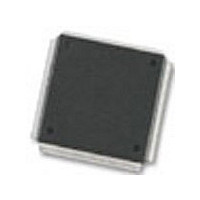
MC68376BAMFT20 Freescale Semiconductor, MC68376BAMFT20 Datasheet - Page 191

MC68376BAMFT20
Manufacturer Part Number
MC68376BAMFT20
Description
Manufacturer
Freescale Semiconductor
Datasheet
1.MC68376BAMFT20.pdf
(434 pages)
Specifications of MC68376BAMFT20
Cpu Family
68K/M683xx
Device Core
ColdFire
Device Core Size
32b
Frequency (max)
20MHz
Interface Type
QSPI/SCI
Program Memory Type
ROM
Program Memory Size
8KB
Total Internal Ram Size
7.5KB
# I/os (max)
18
Number Of Timers - General Purpose
2
Operating Supply Voltage (typ)
5V
Operating Supply Voltage (max)
5.25V
Operating Supply Voltage (min)
4.75V
On-chip Adc
16-chx10-bit
Instruction Set Architecture
RISC
Operating Temp Range
-40C to 125C
Operating Temperature Classification
Automotive
Mounting
Surface Mount
Pin Count
160
Package Type
PQFP
Lead Free Status / Rohs Status
Not Compliant
Available stocks
Company
Part Number
Manufacturer
Quantity
Price
Company:
Part Number:
MC68376BAMFT20
Manufacturer:
FREESCAL
Quantity:
245
- Current page: 191 of 434
- Download datasheet (7Mb)
8.8.1 Port Data Register
8.8.2 Port Data Direction Register
MC68336/376
USER’S MANUAL
There are two special cases to consider for digital I/O port operation. When the MUX
(externally multiplexed) bit is set in QACR0, the data direction register settings are ig-
nored for the bits corresponding to PQA[2:0], the three multiplexed address MA[2:0]
output pins. The MA[2:0] pins are forced to be digital outputs, regardless of the data
direction setting, and the multiplexed address outputs are driven. The data returned
during a port data register read is the value of the multiplexed address latches which
drive MA[2:0], regardless of the data direction setting.
Similarly, when an external trigger queue operating mode is selected, the data direc-
tion register setting for the corresponding pins, PQA3 and/or PQA4, is ignored. The
port pins are forced to be digital inputs for ETRIG1 and/or ETRIG2. The data read
during a port data register read is the actual value of the pin, regardless of the data
direction register setting.
QADC ports A and B are accessed through two 8-bit port data registers (PORTQA and
PORTQB). Port A pins are referred to as PQA[7:0] when used as an 8-bit input/output
port. Port A can also be used for analog inputs AN[59:52], external trigger inputs
ETRIG[2:1], and external multiplexer address outputs MA[2:0].
Port B pins are referred to as PQB[7:0] when used as an 8-bit input-only digital port.
Port B can also be used for non-multiplexed AN[51:48]/AN[3:0] and multiplexed ANz,
ANy, ANx, ANw analog inputs.
PORTQA and PORTQB are unaffected by reset. Refer to D.5.4 Port A/B Data Reg-
ister for register and bit descriptions.
The port data direction register (DDRQA) is associated with the port A digital I/O pins.
These bidirectional pins have somewhat higher leakage and capacitance specifica-
tions. Refer to APPENDIX A ELECTRICAL CHARACTERISTICS for more informa-
tion.
Any bit in this register set to one configures the corresponding pin as an output. Any
bit in this register cleared to zero configures the corresponding pin as an input. Soft-
ware is responsible for ensuring that DDRQA bits are not set to one on pins used for
analog inputs. When a DDRQA bit is set to one and the pin is selected for analog
conversion, the voltage sampled is that of the output digital driver as influenced by the
load.
Since port B is input-only, a data direction register is not needed. Read operations on
the reserved bits in DDRQA return zeros, and writes have no effect. Refer to D.5.5
Port Data Direction Register for register and bit descriptions.
Caution should be exercised when mixing digital and analog inputs.
This should be minimized as much as possible. Input pin rise and fall
times should be as large as possible to minimize AC coupling effects.
QUEUED ANALOG-TO-DIGITAL CONVERTER MODULE
NOTE
MOTOROLA
8-9
Related parts for MC68376BAMFT20
Image
Part Number
Description
Manufacturer
Datasheet
Request
R
Part Number:
Description:
Manufacturer:
Freescale Semiconductor, Inc
Datasheet:
Part Number:
Description:
Manufacturer:
Freescale Semiconductor, Inc
Datasheet:
Part Number:
Description:
Manufacturer:
Freescale Semiconductor, Inc
Datasheet:
Part Number:
Description:
Manufacturer:
Freescale Semiconductor, Inc
Datasheet:
Part Number:
Description:
Manufacturer:
Freescale Semiconductor, Inc
Datasheet:
Part Number:
Description:
Manufacturer:
Freescale Semiconductor, Inc
Datasheet:
Part Number:
Description:
Manufacturer:
Freescale Semiconductor, Inc
Datasheet:
Part Number:
Description:
Manufacturer:
Freescale Semiconductor, Inc
Datasheet:
Part Number:
Description:
Manufacturer:
Freescale Semiconductor, Inc
Datasheet:
Part Number:
Description:
Manufacturer:
Freescale Semiconductor, Inc
Datasheet:
Part Number:
Description:
Manufacturer:
Freescale Semiconductor, Inc
Datasheet:
Part Number:
Description:
Manufacturer:
Freescale Semiconductor, Inc
Datasheet:
Part Number:
Description:
Manufacturer:
Freescale Semiconductor, Inc
Datasheet:
Part Number:
Description:
Manufacturer:
Freescale Semiconductor, Inc
Datasheet:
Part Number:
Description:
Manufacturer:
Freescale Semiconductor, Inc
Datasheet:


