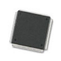
MC68376BAMFT20 Freescale Semiconductor, MC68376BAMFT20 Datasheet - Page 148

MC68376BAMFT20
Manufacturer Part Number
MC68376BAMFT20
Description
Manufacturer
Freescale Semiconductor
Datasheet
1.MC68376BAMFT20.pdf
(434 pages)
Specifications of MC68376BAMFT20
Cpu Family
68K/M683xx
Device Core
ColdFire
Device Core Size
32b
Frequency (max)
20MHz
Interface Type
QSPI/SCI
Program Memory Type
ROM
Program Memory Size
8KB
Total Internal Ram Size
7.5KB
# I/os (max)
18
Number Of Timers - General Purpose
2
Operating Supply Voltage (typ)
5V
Operating Supply Voltage (max)
5.25V
Operating Supply Voltage (min)
4.75V
On-chip Adc
16-chx10-bit
Instruction Set Architecture
RISC
Operating Temp Range
-40C to 125C
Operating Temperature Classification
Automotive
Mounting
Surface Mount
Pin Count
160
Package Type
PQFP
Lead Free Status / Rohs Status
Not Compliant
Available stocks
Company
Part Number
Manufacturer
Quantity
Price
Company:
Part Number:
MC68376BAMFT20
Manufacturer:
FREESCAL
Quantity:
245
- Current page: 148 of 434
- Download datasheet (7Mb)
7.3 MRM Array Address Space Type
7.4 Normal Access
7-2
MOTOROLA
ASPC[1:0] in MRMCR determines ROM array address space type. The module can
respond to both program and data space accesses or to program space accesses
only. This allows code to be executed from ROM, and permits use of program counter
relative addressing mode for operand fetches from the array. The default value of
ASPC[1:0] is established during mask programming, but field value can be changed
after reset if the LOCK bit in the MRMCR has not been masked to a value of one.
Table 7-1 shows ASPC[1:0] field encodings.
Refer to 4.5 Addressing Modes for more information on addressing modes. Refer to
5.5.1.7 Function Codes for more information concerning address space types and
program/data space access.
The array can be accessed by byte, word, or long word. A byte or aligned word access
takes a minimum of one bus cycle (two system clocks). A long word access requires
two bus cycles. Misaligned accesses are not permitted by the CPU32 and will result in
an address error exception.
Access time can be optimized for a particular application by inserting wait states into
each access. The number of wait states inserted is determined by the value of
WAIT[1:0] in the MRMCR. Two, three, four, or five bus-cycle accesses can be speci-
fied. The default value WAIT[1:0] is established during mask programming, but field
value can be changed after reset if the LOCK bit in the MRMCR has not been masked
to a value of one.
Table 7-2 shows WAIT[1:0] field encodings.
Refer to 5.6 Bus Operation for more information concerning access times.
ASPC[1:0]
Table 7-1 ROM Array Space Type
WAIT[1:0]
00
01
10
11
00
01
10
11
Table 7-2 Wait States Field
MASKED ROM MODULE
Unrestricted program and data
Supervisor program and data
Cycles per Transfer
Unrestricted program
Supervisor program
State Specified
3
4
5
2
USER’S MANUAL
MC68336/376
Related parts for MC68376BAMFT20
Image
Part Number
Description
Manufacturer
Datasheet
Request
R
Part Number:
Description:
Manufacturer:
Freescale Semiconductor, Inc
Datasheet:
Part Number:
Description:
Manufacturer:
Freescale Semiconductor, Inc
Datasheet:
Part Number:
Description:
Manufacturer:
Freescale Semiconductor, Inc
Datasheet:
Part Number:
Description:
Manufacturer:
Freescale Semiconductor, Inc
Datasheet:
Part Number:
Description:
Manufacturer:
Freescale Semiconductor, Inc
Datasheet:
Part Number:
Description:
Manufacturer:
Freescale Semiconductor, Inc
Datasheet:
Part Number:
Description:
Manufacturer:
Freescale Semiconductor, Inc
Datasheet:
Part Number:
Description:
Manufacturer:
Freescale Semiconductor, Inc
Datasheet:
Part Number:
Description:
Manufacturer:
Freescale Semiconductor, Inc
Datasheet:
Part Number:
Description:
Manufacturer:
Freescale Semiconductor, Inc
Datasheet:
Part Number:
Description:
Manufacturer:
Freescale Semiconductor, Inc
Datasheet:
Part Number:
Description:
Manufacturer:
Freescale Semiconductor, Inc
Datasheet:
Part Number:
Description:
Manufacturer:
Freescale Semiconductor, Inc
Datasheet:
Part Number:
Description:
Manufacturer:
Freescale Semiconductor, Inc
Datasheet:
Part Number:
Description:
Manufacturer:
Freescale Semiconductor, Inc
Datasheet:


