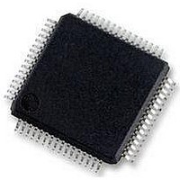
MC56F8257MLH Freescale Semiconductor, MC56F8257MLH Datasheet - Page 356

MC56F8257MLH
Manufacturer Part Number
MC56F8257MLH
Description
DSC 64K FLASH 60MHZ 64-LQFP
Manufacturer
Freescale Semiconductor
Series
56F8xxxr
Datasheets
1.TWR-56F8257.pdf
(88 pages)
2.MC56F8245VLD.pdf
(14 pages)
3.MC56F8245VLD.pdf
(2 pages)
4.MC56F8245VLD.pdf
(629 pages)
Specifications of MC56F8257MLH
Core Processor
56800E
Core Size
16-Bit
Speed
60MHz
Connectivity
CAN, I²C, LIN, SCI, SPI
Peripherals
LVD, POR, PWM, WDT
Number Of I /o
54
Program Memory Size
64KB (32K x 16)
Program Memory Type
FLASH
Ram Size
4K x 16
Voltage - Supply (vcc/vdd)
3 V ~ 3.6 V
Data Converters
A/D 16x12b, D/A 1x12b
Oscillator Type
Internal
Operating Temperature
-40°C ~ 105°C
Package / Case
64-LQFP
Product
DSCs
Processor Series
56800E
Core
56800E
Device Million Instructions Per Second
60 MIPs
Maximum Clock Frequency
60 MHz
Number Of Programmable I/os
54
Data Ram Size
8 KB
Operating Supply Voltage
3.3 V
Maximum Operating Temperature
+ 105 C
Mounting Style
SMD/SMT
Minimum Operating Temperature
- 40 C
On-chip Adc
12 bit, 8 Channel
Lead Free Status / RoHS Status
Lead free / RoHS Compliant
Eeprom Size
-
Lead Free Status / Rohs Status
Details
Available stocks
Company
Part Number
Manufacturer
Quantity
Price
Company:
Part Number:
MC56F8257MLH
Manufacturer:
MOTOLOLA
Quantity:
560
Company:
Part Number:
MC56F8257MLH
Manufacturer:
Freescale Semiconductor
Quantity:
10 000
- TWR-56F8257 PDF datasheet
- MC56F8245VLD PDF datasheet #2
- MC56F8245VLD PDF datasheet #3
- MC56F8245VLD PDF datasheet #4
- Current page: 356 of 629
- Download datasheet (4Mb)
Memory Map and Registers
356
RSRC
WAKE
TEIE
Field
POL
PE
PT
13
12
11
10
M
9
8
7
0
1
Receiver Source
When CTRL1[LOOP]=1, CTRL1[RSRC] determines the internal feedback path for the receiver.
0
1
Data Format Mode
This bit determines whether data characters are eight or nine bits long.
0
1
Wake-up Condition
This bit determines which condition wakes the SCI: a one (address mark) in the most significant bit
position of a received data character or an idle condition on the RXD pin.
0
1
Polarity
This bit determines whether to invert the data as it goes from the transmitter to the TXD pin and from the
RXD pin to the receiver. All bits (start, data, and stop) are inverted as they leave the transmit shift register
and before they enter the receive shift register.
NOTE: It is recommended that CTRL1[POL] be toggled only when CTRL1[TE]=0 and CTRL1[RE]=0.
0
1
Parity Enable
This bit enables the parity function. When enabled, the parity function replaces the most significant bit of
the data character with a parity bit.
0
1
Parity Type
This bit determines whether the SCI generates and checks for even parity or odd parity of the data bits.
With even parity, an even number of ones clears the parity bit and an odd number of ones sets the parity
bit. With odd parity, an odd number of ones clears the parity bit and an even number of ones sets the
parity bit.
0
1
Transmitter Empty Interrupt Enable
This bit enables the transmit data register empty flag, STAT[TDRE], to generate interrupt requests.
SCI enabled in wait mode
SCI disabled in wait mode
Receiver input internally connected to transmitter output
Receiver input connected to TXD pin
One start bit, eight data bits, one stop bit
One start bit, nine data bits, one stop bit
Idle line wake-up
Address mark wake-up
Don’t invert transmit and receive data bits (normal mode)
Invert transmit and receive data bits (inverted mode)
Parity function disabled
Parity function enabled
Even parity
Odd parity
QSCIx_CTRL1 field descriptions (continued)
MC56F825x/4x Reference Manual, Rev. 2, 10/2010
Table continues on the next page...
Preliminary
Description
Freescale Semiconductor
Related parts for MC56F8257MLH
Image
Part Number
Description
Manufacturer
Datasheet
Request
R
Part Number:
Description:
Manufacturer:
Freescale Semiconductor, Inc
Datasheet:
Part Number:
Description:
Manufacturer:
Freescale Semiconductor, Inc
Datasheet:
Part Number:
Description:
Manufacturer:
Freescale Semiconductor, Inc
Datasheet:
Part Number:
Description:
Manufacturer:
Freescale Semiconductor, Inc
Datasheet:
Part Number:
Description:
Manufacturer:
Freescale Semiconductor, Inc
Datasheet:
Part Number:
Description:
Manufacturer:
Freescale Semiconductor, Inc
Datasheet:
Part Number:
Description:
Manufacturer:
Freescale Semiconductor, Inc
Datasheet:
Part Number:
Description:
Manufacturer:
Freescale Semiconductor, Inc
Datasheet:
Part Number:
Description:
Manufacturer:
Freescale Semiconductor, Inc
Datasheet:
Part Number:
Description:
Manufacturer:
Freescale Semiconductor, Inc
Datasheet:
Part Number:
Description:
Manufacturer:
Freescale Semiconductor, Inc
Datasheet:
Part Number:
Description:
Manufacturer:
Freescale Semiconductor, Inc
Datasheet:
Part Number:
Description:
Manufacturer:
Freescale Semiconductor, Inc
Datasheet:
Part Number:
Description:
Manufacturer:
Freescale Semiconductor, Inc
Datasheet:
Part Number:
Description:
Manufacturer:
Freescale Semiconductor, Inc
Datasheet:


