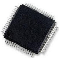
MC56F8257MLH Freescale Semiconductor, MC56F8257MLH Datasheet - Page 94

MC56F8257MLH
Manufacturer Part Number
MC56F8257MLH
Description
DSC 64K FLASH 60MHZ 64-LQFP
Manufacturer
Freescale Semiconductor
Series
56F8xxxr
Datasheets
1.TWR-56F8257.pdf
(88 pages)
2.MC56F8245VLD.pdf
(14 pages)
3.MC56F8245VLD.pdf
(2 pages)
4.MC56F8245VLD.pdf
(629 pages)
Specifications of MC56F8257MLH
Core Processor
56800E
Core Size
16-Bit
Speed
60MHz
Connectivity
CAN, I²C, LIN, SCI, SPI
Peripherals
LVD, POR, PWM, WDT
Number Of I /o
54
Program Memory Size
64KB (32K x 16)
Program Memory Type
FLASH
Ram Size
4K x 16
Voltage - Supply (vcc/vdd)
3 V ~ 3.6 V
Data Converters
A/D 16x12b, D/A 1x12b
Oscillator Type
Internal
Operating Temperature
-40°C ~ 105°C
Package / Case
64-LQFP
Product
DSCs
Processor Series
56800E
Core
56800E
Device Million Instructions Per Second
60 MIPs
Maximum Clock Frequency
60 MHz
Number Of Programmable I/os
54
Data Ram Size
8 KB
Operating Supply Voltage
3.3 V
Maximum Operating Temperature
+ 105 C
Mounting Style
SMD/SMT
Minimum Operating Temperature
- 40 C
On-chip Adc
12 bit, 8 Channel
Lead Free Status / RoHS Status
Lead free / RoHS Compliant
Eeprom Size
-
Lead Free Status / Rohs Status
Details
Available stocks
Company
Part Number
Manufacturer
Quantity
Price
Company:
Part Number:
MC56F8257MLH
Manufacturer:
MOTOLOLA
Quantity:
560
Company:
Part Number:
MC56F8257MLH
Manufacturer:
Freescale Semiconductor
Quantity:
10 000
- TWR-56F8257 PDF datasheet
- MC56F8245VLD PDF datasheet #2
- MC56F8245VLD PDF datasheet #3
- MC56F8245VLD PDF datasheet #4
- Current page: 94 of 629
- Download datasheet (4Mb)
Reset
2.5 Reset
At reset, all the registers return to the reset state. The source of the single RST signal is
the SIM.
2.6 Clocks
The ADC has two external clock inputs to drive two clock domains within the ADC
module.
The IP_CLK is enabled only when the SIM_PCE[ADC] bit is set. This clock enable bit
must be set before the ADC can be used.
The conversion clock is the primary source for the ADC clock and is always selected as
the ADC clock when conversions are in process. The clock source controls in the OCCS
(PRECS, ROPD, ROSB), and CTRL2[DIV0] and PWR2[DIV1] should be configured so
that conversion clock frequency falls between 100 kHz and 15 MHz. Operating the ADC
at out-of-spec conversion clock frequencies or reconfiguring the parameters that affect
clock rates or power modes while the regulators are powered up (PWR[PD0]=0 or
PWR[PD1]=0) negatively affects conversion accuracy.
The conversion clock that the ADC uses for sampling is calculated using the IP bus clock
and the clock divisor bits within the ADC Control Register 2. The ADC clock is active
100 percent of the time in looping modes or in normal power mode. It is also active
during all ADC powerup sequences for a period of time determined by the
PWR[PUDELAY] field. If a conversion is initiated in power savings mode, then the
ADC clock continues until the conversion sequence completes.
The following diagram shows the structure of the clocking system.
94
Clock input
adc_8_clk
IP Clock
ROSC clock
MC56F825x/4x Reference Manual, Rev. 2, 10/2010
Source
SIM
Table 2-69. Clock Summary
Maximum rate is 60 MHz. When the PLL is on and selected, it is PLL out‐
put divided by 4. When PLL is not selected, it is MSTR_OSC/2. When the
device is in low-power mode, ROSB=1, the rate is 200 kHz.
ROSC provides 8 MHz for auto-standby power saving mode.
Characteristics
Preliminary
Freescale Semiconductor
Related parts for MC56F8257MLH
Image
Part Number
Description
Manufacturer
Datasheet
Request
R
Part Number:
Description:
Manufacturer:
Freescale Semiconductor, Inc
Datasheet:
Part Number:
Description:
Manufacturer:
Freescale Semiconductor, Inc
Datasheet:
Part Number:
Description:
Manufacturer:
Freescale Semiconductor, Inc
Datasheet:
Part Number:
Description:
Manufacturer:
Freescale Semiconductor, Inc
Datasheet:
Part Number:
Description:
Manufacturer:
Freescale Semiconductor, Inc
Datasheet:
Part Number:
Description:
Manufacturer:
Freescale Semiconductor, Inc
Datasheet:
Part Number:
Description:
Manufacturer:
Freescale Semiconductor, Inc
Datasheet:
Part Number:
Description:
Manufacturer:
Freescale Semiconductor, Inc
Datasheet:
Part Number:
Description:
Manufacturer:
Freescale Semiconductor, Inc
Datasheet:
Part Number:
Description:
Manufacturer:
Freescale Semiconductor, Inc
Datasheet:
Part Number:
Description:
Manufacturer:
Freescale Semiconductor, Inc
Datasheet:
Part Number:
Description:
Manufacturer:
Freescale Semiconductor, Inc
Datasheet:
Part Number:
Description:
Manufacturer:
Freescale Semiconductor, Inc
Datasheet:
Part Number:
Description:
Manufacturer:
Freescale Semiconductor, Inc
Datasheet:
Part Number:
Description:
Manufacturer:
Freescale Semiconductor, Inc
Datasheet:


