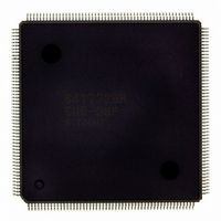
D6417729RHF200BV Renesas Electronics America, D6417729RHF200BV Datasheet - Page 340

D6417729RHF200BV
Manufacturer Part Number
D6417729RHF200BV
Description
IC SUPER H MPU ROMLESS 208QFP
Manufacturer
Renesas Electronics America
Series
SuperH® SH7700r
Datasheet
1.D6417729RF133BV.pdf
(857 pages)
Specifications of D6417729RHF200BV
Core Processor
SH-3 DSP
Core Size
32-Bit
Speed
200MHz
Connectivity
EBI/EMI, FIFO, IrDA, SCI, SmartCard
Peripherals
DMA, POR, WDT
Number Of I /o
96
Program Memory Type
ROMless
Ram Size
32K x 8
Voltage - Supply (vcc/vdd)
1.85 V ~ 2.15 V
Data Converters
A/D 8x10b; D/A 2x8b
Oscillator Type
Internal
Operating Temperature
-20°C ~ 75°C
Package / Case
208-QFP Exposed Pad, 208-eQFP, 208-HQFP
Lead Free Status / RoHS Status
Lead free / RoHS Compliant
Eeprom Size
-
Program Memory Size
-
Available stocks
Company
Part Number
Manufacturer
Quantity
Price
Company:
Part Number:
D6417729RHF200BV
Manufacturer:
EVERLIGHT
Quantity:
1 000
Company:
Part Number:
D6417729RHF200BV
Manufacturer:
Renesas Electronics America
Quantity:
10 000
- Current page: 340 of 857
- Download datasheet (5Mb)
Bits 13 and 12—RAS–CAS Delay (RCD1, RCD0): When synchronous DRAM interface is
selected as connected memory, these bits set the bank active read/write command delay time.
Bit 13: RCD1
0
1
Bits 11 and 10—Write-Precharge Delay (TRWL1, TRWL0): Set the synchronous DRAM
write-precharge delay time. This designates the time between the end of a write cycle and the next
bank-active command. This setting is valid only when synchronous DRAM is connected. After the
write cycle, the next bank-active command is not issued for the period TPC + TRWL.
Bit 11: TRWL1
0
1
Bits 9 and 8—C C C C A A A A S S S S -Before-R R R R A A A A S S S S Refresh R R R R A A A A S S S S Assert Time (TRAS1, TRAS0): When
synchronous DRAM interface is selected as a connected memory, no bank-active command is
issued during the period TPC + TRAS after an auto-refresh command.
Bit 9: TRAS1
0
1
Bit 7—Synchronous DRAM Bank Active (RASD): Specifies whether synchronous DRAM is
used in bank active mode or auto-precharge mode. Set auto-precharge mode when areas 2 and 3
are both designated as synchronous DRAM space. The bank active mode should not be used
unless the bus width for all areas is 32 bits.
Bit 7: RASD
0
1
Rev. 5.0, 09/03, page 292 of 806
Bit 12: RCD0
0
1
0
1
Bit 10: TRWL0
0
1
0
1
Bit 8: TRAS0
0
1
0
1
Description
Auto-precharge mode
Bank active mode
Description
1 cycle
2 cycles
3 cycles
4 cycles
Description
1 cycle
2 cycles
3 cycles
Reserved (Setting prohibited)
Description
2 cycles
3 cycles
4 cycles
5 cycles
(Initial value)
(Initial value)
(Initial value)
(Initial value)
Related parts for D6417729RHF200BV
Image
Part Number
Description
Manufacturer
Datasheet
Request
R

Part Number:
Description:
KIT STARTER FOR M16C/29
Manufacturer:
Renesas Electronics America
Datasheet:

Part Number:
Description:
KIT STARTER FOR R8C/2D
Manufacturer:
Renesas Electronics America
Datasheet:

Part Number:
Description:
R0K33062P STARTER KIT
Manufacturer:
Renesas Electronics America
Datasheet:

Part Number:
Description:
KIT STARTER FOR R8C/23 E8A
Manufacturer:
Renesas Electronics America
Datasheet:

Part Number:
Description:
KIT STARTER FOR R8C/25
Manufacturer:
Renesas Electronics America
Datasheet:

Part Number:
Description:
KIT STARTER H8S2456 SHARPE DSPLY
Manufacturer:
Renesas Electronics America
Datasheet:

Part Number:
Description:
KIT STARTER FOR R8C38C
Manufacturer:
Renesas Electronics America
Datasheet:

Part Number:
Description:
KIT STARTER FOR R8C35C
Manufacturer:
Renesas Electronics America
Datasheet:

Part Number:
Description:
KIT STARTER FOR R8CL3AC+LCD APPS
Manufacturer:
Renesas Electronics America
Datasheet:

Part Number:
Description:
KIT STARTER FOR RX610
Manufacturer:
Renesas Electronics America
Datasheet:

Part Number:
Description:
KIT STARTER FOR R32C/118
Manufacturer:
Renesas Electronics America
Datasheet:

Part Number:
Description:
KIT DEV RSK-R8C/26-29
Manufacturer:
Renesas Electronics America
Datasheet:

Part Number:
Description:
KIT STARTER FOR SH7124
Manufacturer:
Renesas Electronics America
Datasheet:

Part Number:
Description:
KIT STARTER FOR H8SX/1622
Manufacturer:
Renesas Electronics America
Datasheet:

Part Number:
Description:
KIT DEV FOR SH7203
Manufacturer:
Renesas Electronics America
Datasheet:


