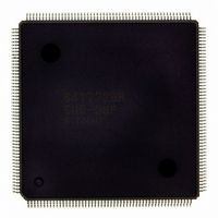
D6417729RHF200BV Renesas Electronics America, D6417729RHF200BV Datasheet - Page 78

D6417729RHF200BV
Manufacturer Part Number
D6417729RHF200BV
Description
IC SUPER H MPU ROMLESS 208QFP
Manufacturer
Renesas Electronics America
Series
SuperH® SH7700r
Datasheet
1.D6417729RF133BV.pdf
(857 pages)
Specifications of D6417729RHF200BV
Core Processor
SH-3 DSP
Core Size
32-Bit
Speed
200MHz
Connectivity
EBI/EMI, FIFO, IrDA, SCI, SmartCard
Peripherals
DMA, POR, WDT
Number Of I /o
96
Program Memory Type
ROMless
Ram Size
32K x 8
Voltage - Supply (vcc/vdd)
1.85 V ~ 2.15 V
Data Converters
A/D 8x10b; D/A 2x8b
Oscillator Type
Internal
Operating Temperature
-20°C ~ 75°C
Package / Case
208-QFP Exposed Pad, 208-eQFP, 208-HQFP
Lead Free Status / RoHS Status
Lead free / RoHS Compliant
Eeprom Size
-
Program Memory Size
-
Available stocks
Company
Part Number
Manufacturer
Quantity
Price
Company:
Part Number:
D6417729RHF200BV
Manufacturer:
EVERLIGHT
Quantity:
1 000
Company:
Part Number:
D6417729RHF200BV
Manufacturer:
Renesas Electronics America
Quantity:
10 000
- Current page: 78 of 857
- Download datasheet (5Mb)
2.1.3
The SH7729R has four system registers, MACL, MACH, PR, and PC (figure 2.6).
The DSR, A0, X0, X1, Y0, and Y1 registers are also treated as system registers. Therefore,
instructions for data transfer between general registers and system registers are supported for these
registers.
2.1.4
The SH7729R has eight data registers and one status register as DSP registers (figure 2.7). The
data registers are 32-bit width with the exception of registers A0 and A1. Registers A0 and A1
include 8 guard bits (fields A0G and A1G), giving them a total width of 40 bits.
Three kinds of operation access the DSP data registers. The first is DSP data processing. When a
DSP fixed-point data operation uses A0 or A1 as the source register, it uses the guard bits (bits
39–32). When it uses A0 or A1 as the destination register, guard bits 39–32 are valid. When a DSP
fixed-point data operation uses a DSP register other than A0 or A1 as the source register, it sign-
extends the source value to bits 39–32. When it uses one of these registers as the destination
register, bits 39–32 of the result are discarded.
The second kind of operation is an X or Y data transfer operation,
operation accesses the X and Y memories through the 16-bit X and Y data buses (figure 2.8). The
register to be loaded or stored by this operation always comprises the upper 16 bits (bits 31–16).
X0 or X1 can be the destination of an X memory load and Y0 or Y1 can be the destination of a Y
memory load, but no other register can be the destination register in this operation. When data is
read into the upper 16 bits of a register (bits 31–16), the lower 16 bits of the register (bits 15–0)
are automatically cleared.
A0 and A1 can be stored in the X or Y memory using the X or Y data transfer instructions
MOVX.W and MOVY.W, but no other registers can be stored.
Rev. 5.0, 09/03, page 30 of 806
31
31
31
System Registers
DSP Registers
MACH
MACL
PR
PC
Figure 2.6 System Registers
0
0
0
Multiply and accumulate high and low registers
(MACH/L)
Store the results of multiplicationand accumulation
operations.
Procedure register (PR)
Stores the subroutine procedure return address.
Program counter (PC)
Indicates the start address of the current instruction.
“
MOVX.W MOVY.W”. This
Related parts for D6417729RHF200BV
Image
Part Number
Description
Manufacturer
Datasheet
Request
R

Part Number:
Description:
KIT STARTER FOR M16C/29
Manufacturer:
Renesas Electronics America
Datasheet:

Part Number:
Description:
KIT STARTER FOR R8C/2D
Manufacturer:
Renesas Electronics America
Datasheet:

Part Number:
Description:
R0K33062P STARTER KIT
Manufacturer:
Renesas Electronics America
Datasheet:

Part Number:
Description:
KIT STARTER FOR R8C/23 E8A
Manufacturer:
Renesas Electronics America
Datasheet:

Part Number:
Description:
KIT STARTER FOR R8C/25
Manufacturer:
Renesas Electronics America
Datasheet:

Part Number:
Description:
KIT STARTER H8S2456 SHARPE DSPLY
Manufacturer:
Renesas Electronics America
Datasheet:

Part Number:
Description:
KIT STARTER FOR R8C38C
Manufacturer:
Renesas Electronics America
Datasheet:

Part Number:
Description:
KIT STARTER FOR R8C35C
Manufacturer:
Renesas Electronics America
Datasheet:

Part Number:
Description:
KIT STARTER FOR R8CL3AC+LCD APPS
Manufacturer:
Renesas Electronics America
Datasheet:

Part Number:
Description:
KIT STARTER FOR RX610
Manufacturer:
Renesas Electronics America
Datasheet:

Part Number:
Description:
KIT STARTER FOR R32C/118
Manufacturer:
Renesas Electronics America
Datasheet:

Part Number:
Description:
KIT DEV RSK-R8C/26-29
Manufacturer:
Renesas Electronics America
Datasheet:

Part Number:
Description:
KIT STARTER FOR SH7124
Manufacturer:
Renesas Electronics America
Datasheet:

Part Number:
Description:
KIT STARTER FOR H8SX/1622
Manufacturer:
Renesas Electronics America
Datasheet:

Part Number:
Description:
KIT DEV FOR SH7203
Manufacturer:
Renesas Electronics America
Datasheet:


