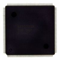
D6417729RHF200BV Renesas Electronics America, D6417729RHF200BV Datasheet - Page 36

D6417729RHF200BV
Manufacturer Part Number
D6417729RHF200BV
Description
IC SUPER H MPU ROMLESS 208QFP
Manufacturer
Renesas Electronics America
Series
SuperH® SH7700r
Datasheet
1.D6417729RF133BV.pdf
(857 pages)
Specifications of D6417729RHF200BV
Core Processor
SH-3 DSP
Core Size
32-Bit
Speed
200MHz
Connectivity
EBI/EMI, FIFO, IrDA, SCI, SmartCard
Peripherals
DMA, POR, WDT
Number Of I /o
96
Program Memory Type
ROMless
Ram Size
32K x 8
Voltage - Supply (vcc/vdd)
1.85 V ~ 2.15 V
Data Converters
A/D 8x10b; D/A 2x8b
Oscillator Type
Internal
Operating Temperature
-20°C ~ 75°C
Package / Case
208-QFP Exposed Pad, 208-eQFP, 208-HQFP
Lead Free Status / RoHS Status
Lead free / RoHS Compliant
Eeprom Size
-
Program Memory Size
-
Available stocks
Company
Part Number
Manufacturer
Quantity
Price
Company:
Part Number:
D6417729RHF200BV
Manufacturer:
EVERLIGHT
Quantity:
1 000
Company:
Part Number:
D6417729RHF200BV
Manufacturer:
Renesas Electronics America
Quantity:
10 000
- Current page: 36 of 857
- Download datasheet (5Mb)
Figure 5.5
Figure 5.6
Figure 6.1
Figure 6.2
Figure 7.1
Figure 7.2
Figure 7.3
Figure 7.4
Figure 8.1
Figure 8.2
Figure 9.1
Figure 9.2
Figure 9.3
Figure 9.4
Figure 9.5
Figure 9.6
Figure 9.7
Figure 9.8
Figure 9.9
Figure 9.10
Figure 9.11
Figure 10.1
Figure 10.2
Figure 10.3
Figure 10.4
Figure 10.5
Figure 11.1
Figure 11.2
Figure 11.3
Figure 11.4
Figure 11.5
Figure 11.6
Figure 11.7
Figure 11.8
Figure 11.9
Figure 11.10 Basic Interface Wait Timing (Software Wait Only)............................................. 319
Figure 11.11 Basic Interface Wait State Timing (Wait State Insertion by WAIT Signal
Figure 11.12 Example of 64-Mbit Synchronous DRAM Connection (32-Bit Bus Width)........ 322
Figure 11.13 Example of 64-Mbit Synchronous DRAM (16-Bit Bus Width) ........................... 323
Figure 11.14 Basic Timing for Synchronous DRAM Burst Read ............................................. 326
Figure 11.15 Synchronous DRAM Burst Read Wait Specification Timing .............................. 327
Rev. 5.0, 09/03, page xxxiv of xlvi
Write-Back Buffer Configuration......................................................................... 150
Specifying Address and Data for Memory-Mapped Cache Access...................... 153
X/Y Memory Logical Address Mapping.............................................................. 159
X/Y Memory Physical Address Mapping ............................................................ 160
Block Diagram of INTC....................................................................................... 162
Example of IRL Interrupt Connection.................................................................. 166
Interrupt Operation Flowchart .............................................................................. 188
Example of Pipeline Operations when IRL Interrupt is Accepted ....................... 192
Block Diagram of User Break Controller............................................................. 195
When Interrupt Occurs before Branch Instruction is Executed ............................ 218
Canceling Standby Mode with STBCR.STBY..................................................... 235
Power-On Reset (Clock Modes 0, 1, 2, and 7) STATUS Output ......................... 238
Manual Reset STATUS Output............................................................................ 239
Standby to Interrupt STATUS Output.................................................................. 240
Standby to Power-On Reset STATUS Output...................................................... 241
Standby to Manual Reset STATUS Output.......................................................... 242
Sleep to Interrupt STATUS Output ...................................................................... 243
Sleep to Power-On Reset STATUS Output.......................................................... 243
Sleep to Manual Reset STATUS Output.............................................................. 244
Hardware Standby Mode (When CA Goes Low in Normal Operation)............... 246
Hardware Standby Mode Timing (When CA Goes Low during WDT
Operation on Standby Mode Cancellation) .......................................................... 247
Block Diagram of Clock Pulse Generator ............................................................ 250
Block Diagram of WDT ....................................................................................... 260
Writing to WTCNT and WTCSR......................................................................... 264
Points for Attention when Using Crystal Resonator............................................. 266
Points for Attention when Using PLL Oscillator Circuit ..................................... 267
Block Diagram of Bus State Controller................................................................ 271
Correspondence between Logical Address Space and Physical Address Space .. 275
Physical Space Allocation .................................................................................... 277
PCMCIA Space Allocation .................................................................................. 278
Writing to RFCR, RTCSR, RTCNT, and RTCOR............................................... 303
Basic Timing of Basic Interface ........................................................................... 315
Example of 32-Bit Data-Width Static RAM Connection ..................................... 316
Example of 16-Bit Data-Width Static RAM Connection ..................................... 317
Example of 8-Bit Data-Width Static RAM Connection ....................................... 318
WAITSEL = 1)..................................................................................................... 320
Related parts for D6417729RHF200BV
Image
Part Number
Description
Manufacturer
Datasheet
Request
R

Part Number:
Description:
KIT STARTER FOR M16C/29
Manufacturer:
Renesas Electronics America
Datasheet:

Part Number:
Description:
KIT STARTER FOR R8C/2D
Manufacturer:
Renesas Electronics America
Datasheet:

Part Number:
Description:
R0K33062P STARTER KIT
Manufacturer:
Renesas Electronics America
Datasheet:

Part Number:
Description:
KIT STARTER FOR R8C/23 E8A
Manufacturer:
Renesas Electronics America
Datasheet:

Part Number:
Description:
KIT STARTER FOR R8C/25
Manufacturer:
Renesas Electronics America
Datasheet:

Part Number:
Description:
KIT STARTER H8S2456 SHARPE DSPLY
Manufacturer:
Renesas Electronics America
Datasheet:

Part Number:
Description:
KIT STARTER FOR R8C38C
Manufacturer:
Renesas Electronics America
Datasheet:

Part Number:
Description:
KIT STARTER FOR R8C35C
Manufacturer:
Renesas Electronics America
Datasheet:

Part Number:
Description:
KIT STARTER FOR R8CL3AC+LCD APPS
Manufacturer:
Renesas Electronics America
Datasheet:

Part Number:
Description:
KIT STARTER FOR RX610
Manufacturer:
Renesas Electronics America
Datasheet:

Part Number:
Description:
KIT STARTER FOR R32C/118
Manufacturer:
Renesas Electronics America
Datasheet:

Part Number:
Description:
KIT DEV RSK-R8C/26-29
Manufacturer:
Renesas Electronics America
Datasheet:

Part Number:
Description:
KIT STARTER FOR SH7124
Manufacturer:
Renesas Electronics America
Datasheet:

Part Number:
Description:
KIT STARTER FOR H8SX/1622
Manufacturer:
Renesas Electronics America
Datasheet:

Part Number:
Description:
KIT DEV FOR SH7203
Manufacturer:
Renesas Electronics America
Datasheet:


