D6417729RHF200BV Renesas Electronics America, D6417729RHF200BV Datasheet - Page 44
D6417729RHF200BV
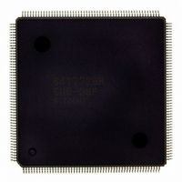
Manufacturer Part Number
D6417729RHF200BV
Description
IC SUPER H MPU ROMLESS 208QFP
Manufacturer
Renesas Electronics America
Series
SuperH® SH7700r
Datasheet
1.D6417729RF133BV.pdf
(857 pages)
Specifications of D6417729RHF200BV
Core Processor
SH-3 DSP
Core Size
32-Bit
Speed
200MHz
Connectivity
EBI/EMI, FIFO, IrDA, SCI, SmartCard
Peripherals
DMA, POR, WDT
Number Of I /o
96
Program Memory Type
ROMless
Ram Size
32K x 8
Voltage - Supply (vcc/vdd)
1.85 V ~ 2.15 V
Data Converters
A/D 8x10b; D/A 2x8b
Oscillator Type
Internal
Operating Temperature
-20°C ~ 75°C
Package / Case
208-QFP Exposed Pad, 208-eQFP, 208-HQFP
Lead Free Status / RoHS Status
Lead free / RoHS Compliant
Eeprom Size
-
Program Memory Size
-
Available stocks
Company
Part Number
Manufacturer
Quantity
Price
Company:

Part Number:
D6417729RHF200BV
Manufacturer:
EVERLIGHT
Quantity:
1 000
Company:
Part Number:
D6417729RHF200BV
Manufacturer:
Renesas Electronics America
Quantity:
10 000


Table 4.4
Table 5.1
Table 5.2
Table 5.3
Table 5.4
Table 5.5
Table 5.6
Table 6.1
Table 7.1
Table 7.2
Table 7.3
Table 7.4
Table 7.5
Table 7.6
Table 7.7
Table 7.8
Table 8.1
Table 8.2
Table 8.3
Table 9.1
Table 9.2
Table 9.3
Table 9.4
Table 10.1
Table 10.2
Table 10.3
Table 10.4
Table 10.5
Table 11.1
Table 11.2
Table 11.3
Table 11.4
Table 11.5
Table 11.6
Table 11.7
Table 11.8
Table 11.9
Table 11.10 32-Bit External Device/Little-Endian Access and Data Alignment........................ 309
Table 11.11 16-Bit External Device/Little-Endian Access and Data Alignment........................ 309
Table 11.12 8-Bit External Device/Little-Endian Access and Data Alignment.......................... 310
Table 11.13 Relationship between Bus Width, AMX Bits, and Address Multiplex Output ....... 324
Rev. 5.0, 09/03, page xlii of xlvi
Types of Reset ........................................................................................................ 133
Cache Specifications............................................................................................... 143
LRU and Way Replacement ................................................................................... 145
Register Configuration............................................................................................ 145
LRU and Way Replacement (when W2LOCK=1) ................................................. 147
LRU and Way Replacement (when W3LOCK=1) ................................................. 147
LRU and Way Replacement (when W2LOCK=1 and W3LOCK=1)..................... 148
X/Y Memory Specifications ................................................................................... 157
INTC Pins ............................................................................................................... 163
INTC Registers ....................................................................................................... 164
IRL3–IRL0/IRLS3–IRLS0 Pins and Interrupt Levels ............................................ 167
Interrupt Exception Handling Sources and Priority (IRQ Mode) ........................... 170
Interrupt Exception Handling Sources and Priority (IRL Mode)............................ 172
Interrupt Levels and INTEVT Codes...................................................................... 174
Interrupt Request Sources and IPRA–IPRE............................................................ 175
Interrupt Response Time......................................................................................... 190
UBC Registers ........................................................................................................ 196
Data Access Cycle Addresses and Operand Size Comparison Conditions............. 216
BSA Values Stored in Exception Handling before Execution of Branch
Destination Instruction............................................................................................ 219
Power-Down Modes ............................................................................................... 228
Pin Configuration.................................................................................................... 229
Register Configuration............................................................................................ 229
Register States in Standby Mode ............................................................................ 234
CPG Pins and Functions ......................................................................................... 252
CPG Register .......................................................................................................... 252
Clock Operating Modes .......................................................................................... 253
Available Combinations of Clock Mode and FRQCR Values................................ 254
Register Configuration............................................................................................ 261
BSC Pins................................................................................................................. 272
BSC Registers......................................................................................................... 274
Physical Address Space Map.................................................................................. 276
Correspondence between External Pins (MD4 and MD3) and Memory Size......... 277
PCMCIA Interface Characteristics ......................................................................... 278
PCMCIA Support Interface .................................................................................... 279
32-Bit External Device/Big-Endian Access and Data Alignment .......................... 306
16-Bit External Device/Big-Endian Access and Data Alignment .......................... 307
8-Bit External Device/Big-Endian Access and Data Alignment ............................ 308
Related parts for D6417729RHF200BV
Image
Part Number
Description
Manufacturer
Datasheet
Request
R

Part Number:
Description:
KIT STARTER FOR M16C/29
Manufacturer:
Renesas Electronics America
Datasheet:

Part Number:
Description:
KIT STARTER FOR R8C/2D
Manufacturer:
Renesas Electronics America
Datasheet:

Part Number:
Description:
R0K33062P STARTER KIT
Manufacturer:
Renesas Electronics America
Datasheet:

Part Number:
Description:
KIT STARTER FOR R8C/23 E8A
Manufacturer:
Renesas Electronics America
Datasheet:

Part Number:
Description:
KIT STARTER FOR R8C/25
Manufacturer:
Renesas Electronics America
Datasheet:

Part Number:
Description:
KIT STARTER H8S2456 SHARPE DSPLY
Manufacturer:
Renesas Electronics America
Datasheet:

Part Number:
Description:
KIT STARTER FOR R8C38C
Manufacturer:
Renesas Electronics America
Datasheet:

Part Number:
Description:
KIT STARTER FOR R8C35C
Manufacturer:
Renesas Electronics America
Datasheet:

Part Number:
Description:
KIT STARTER FOR R8CL3AC+LCD APPS
Manufacturer:
Renesas Electronics America
Datasheet:
Part Number:
Description:
KIT STARTER FOR RX610
Manufacturer:
Renesas Electronics America
Datasheet:

Part Number:
Description:
KIT STARTER FOR R32C/118
Manufacturer:
Renesas Electronics America
Datasheet:

Part Number:
Description:
KIT DEV RSK-R8C/26-29
Manufacturer:
Renesas Electronics America
Datasheet:

Part Number:
Description:
KIT STARTER FOR SH7124
Manufacturer:
Renesas Electronics America
Datasheet:

Part Number:
Description:
KIT STARTER FOR H8SX/1622
Manufacturer:
Renesas Electronics America
Datasheet:

Part Number:
Description:
KIT DEV FOR SH7203
Manufacturer:
Renesas Electronics America
Datasheet: