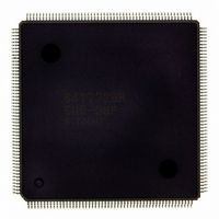
D6417729RHF200BV Renesas Electronics America, D6417729RHF200BV Datasheet - Page 733

D6417729RHF200BV
Manufacturer Part Number
D6417729RHF200BV
Description
IC SUPER H MPU ROMLESS 208QFP
Manufacturer
Renesas Electronics America
Series
SuperH® SH7700r
Datasheet
1.D6417729RF133BV.pdf
(857 pages)
Specifications of D6417729RHF200BV
Core Processor
SH-3 DSP
Core Size
32-Bit
Speed
200MHz
Connectivity
EBI/EMI, FIFO, IrDA, SCI, SmartCard
Peripherals
DMA, POR, WDT
Number Of I /o
96
Program Memory Type
ROMless
Ram Size
32K x 8
Voltage - Supply (vcc/vdd)
1.85 V ~ 2.15 V
Data Converters
A/D 8x10b; D/A 2x8b
Oscillator Type
Internal
Operating Temperature
-20°C ~ 75°C
Package / Case
208-QFP Exposed Pad, 208-eQFP, 208-HQFP
Lead Free Status / RoHS Status
Lead free / RoHS Compliant
Eeprom Size
-
Program Memory Size
-
Available stocks
Company
Part Number
Manufacturer
Quantity
Price
Company:
Part Number:
D6417729RHF200BV
Manufacturer:
EVERLIGHT
Quantity:
1 000
Company:
Part Number:
D6417729RHF200BV
Manufacturer:
Renesas Electronics America
Quantity:
10 000
- Current page: 733 of 857
- Download datasheet (5Mb)
23.1
The SH7729R incorporates a user debugging interface (UDI) and advanced user debugger (AUD)
for program debugging.
23.2
The UDI (user debugging interface) performs on-chip debugging which is supported by the
SH7729R. The UDI described here is a serial interface which is compatible with JTAG (Joint Test
Action Group, IEEE Standard 1149.1 and IEEE Standard Test Access Port and Boundary-Scan
Architecture) specifications.
The UDI in the SH7729R supports a boundary scan mode, and is also used for emulator
connection.
When using an emulator, UDI functions should not be used. Refer to the emulator manual for the
method of connecting the emulator.
23.2.1
TCK: UDI serial data input/output clock pin. Data is serially supplied to the UDI from the data
input pin (TDI), and output from the data output pin (TDO), in synchronization with this clock.
TMS: Mode select input pin. The state of the TAP control circuit is determined by changing this
signal in synchronization with TCK. The protocol complies with the JTAG standard (IEEE Std.
1149.1).
T T T T R R R R S S S S T T T T : UDI reset input pin. Input is accepted asynchronously with respect to TCK, and when low,
the UDI is reset. See section 23.4.2, Reset Configuration, for more information.
TDI: UDI serial data input pin. Data transfer to the UDI is executed by changing this signal in
synchronization with TCK.
TDO: UDI serial data output pin. Data output from the UDI is executed by reading this signal in
synchronization with TCK.
A A A A S S S S E E E E M M M M D D D D 0 0 0 0 : ASE mode select pin. If a low level is input at the ASEMD0 pin while the RESETP
pin is asserted, ASE mode is entered; if a high level is input, normal mode is entered. In ASE
mode, boundary scan and emulator functions can be used. The input level at the ASEMD0 pin
should be held for at least one cycle after RESETP negation.
Overview
User Debugging Interface (UDI)
Pin Descriptions
Section 23 User Debugging Interface (UDI)
Rev. 5.0, 09/03, page 685 of 806
Related parts for D6417729RHF200BV
Image
Part Number
Description
Manufacturer
Datasheet
Request
R

Part Number:
Description:
KIT STARTER FOR M16C/29
Manufacturer:
Renesas Electronics America
Datasheet:

Part Number:
Description:
KIT STARTER FOR R8C/2D
Manufacturer:
Renesas Electronics America
Datasheet:

Part Number:
Description:
R0K33062P STARTER KIT
Manufacturer:
Renesas Electronics America
Datasheet:

Part Number:
Description:
KIT STARTER FOR R8C/23 E8A
Manufacturer:
Renesas Electronics America
Datasheet:

Part Number:
Description:
KIT STARTER FOR R8C/25
Manufacturer:
Renesas Electronics America
Datasheet:

Part Number:
Description:
KIT STARTER H8S2456 SHARPE DSPLY
Manufacturer:
Renesas Electronics America
Datasheet:

Part Number:
Description:
KIT STARTER FOR R8C38C
Manufacturer:
Renesas Electronics America
Datasheet:

Part Number:
Description:
KIT STARTER FOR R8C35C
Manufacturer:
Renesas Electronics America
Datasheet:

Part Number:
Description:
KIT STARTER FOR R8CL3AC+LCD APPS
Manufacturer:
Renesas Electronics America
Datasheet:

Part Number:
Description:
KIT STARTER FOR RX610
Manufacturer:
Renesas Electronics America
Datasheet:

Part Number:
Description:
KIT STARTER FOR R32C/118
Manufacturer:
Renesas Electronics America
Datasheet:

Part Number:
Description:
KIT DEV RSK-R8C/26-29
Manufacturer:
Renesas Electronics America
Datasheet:

Part Number:
Description:
KIT STARTER FOR SH7124
Manufacturer:
Renesas Electronics America
Datasheet:

Part Number:
Description:
KIT STARTER FOR H8SX/1622
Manufacturer:
Renesas Electronics America
Datasheet:

Part Number:
Description:
KIT DEV FOR SH7203
Manufacturer:
Renesas Electronics America
Datasheet:


