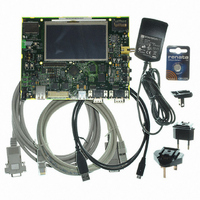
AT91SAM9G45-EKES Atmel, AT91SAM9G45-EKES Datasheet - Page 1099

AT91SAM9G45-EKES
Manufacturer Part Number
AT91SAM9G45-EKES
Description
KIT EVAL FOR AT91SAM9G45
Manufacturer
Atmel
Series
AT91SAM Smart ARMr
Type
MCUr
Datasheets
1.AT91SAM9G45-EKES.pdf
(56 pages)
2.AT91SAM9G45-EKES.pdf
(1218 pages)
3.AT91SAM9G45-EKES.pdf
(66 pages)
Specifications of AT91SAM9G45-EKES
Contents
Board
Processor To Be Evaluated
SAM9G45
Data Bus Width
32 bit
Interface Type
I2C, SPI, UART
Maximum Operating Temperature
+ 50 C
Minimum Operating Temperature
- 10 C
Operating Supply Voltage
1.8 V to 3.3 V
For Use With/related Products
AT91SAM9G45
Lead Free Status / RoHS Status
Lead free / RoHS Compliant
Other names
Q4626953
- Current page: 1099 of 1218
- Download datasheet (19Mb)
45.5.3
45.6
45.6.1
45.6.1.1
45.6.1.2
45.6.1.3
6438F–ATARM–21-Jun-10
Functional Description
Interrupt Sources
DMA Controller
Configuration Block
AHB Interface
Channel-U
The LCD Controller interrupt line is connected to one of the internal sources of the Advanced
Interrupt Controller. Using the LCD Controller interrupt requires prior programming of the AIC.
Table 45-3.
The LCD Controller consists of two main blocks
and the LCD controller core (LCDC core). The DMA controller reads the display data from an
external memory through a AHB master interface. The LCD controller core formats the display
data. The LCD controller core continuously pumps the pixel data into the LCD module via the
LCD data bus (LCDD[23:0]); this bus is timed by the LCDDOTCK, LCDDEN, LCDHSYNC, and
LCDVSYNC signals.
The configuration block is a set of programmable registers that are used to configure the DMA
controller operation. These registers are written via the AHB slave interface. Only word access is
allowed.
For details on the configuration registers, see
1125.
This block generates the AHB transactions. It generates undefined-length incrementing bursts
as well as 4-, 8- or 16-beat incrementing bursts. The size of the transfer can be configured in the
BRSTLN field of the DMAFRMCFG register. For details on this register, see
figuration Register” on page
This block stores the base address and the number of words transferred for this channel (frame
in single scan mode and Upper Panel in dual scan mode) since the beginning of the frame. It
also generates the end of frame signal.
It has two pointers, the base address and the number of words to transfer. When the module
receives a new_frame signal, it reloads the number of words to transfer pointer with the size of
the frame/panel. When the module receives the new_frame signal, it also reloads the base
address with the base address programmed by the host.
The size of the frame/panel can be programmed in the FRMSIZE field of the DMAFRMCFG
Register. This size is calculated as follows:
where:
X_size = ((LINESIZE+1)*Bpp+PIXELOFF)/32
Y_size = (LINEVAL+1)
Instance
LCDC
Peripheral IDs
Frame_size
23
ID
1130.
=
X_size*Y_size
------------------------------------- -
32
“LCD Controller (LCDC) User Interface” on page
(Figure 45-1 on page
AT91SAM9G45
1096), the DMA controller
“DMA Frame Con-
1099
Related parts for AT91SAM9G45-EKES
Image
Part Number
Description
Manufacturer
Datasheet
Request
R

Part Number:
Description:
MCU ARM9 64K SRAM 144-LFBGA
Manufacturer:
Atmel
Datasheet:

Part Number:
Description:
IC ARM7 MCU FLASH 256K 100LQFP
Manufacturer:
Atmel
Datasheet:

Part Number:
Description:
IC ARM9 MPU 217-LFBGA
Manufacturer:
Atmel
Datasheet:

Part Number:
Description:
MCU ARM9 ULTRA LOW PWR 217-LFBGA
Manufacturer:
Atmel
Datasheet:

Part Number:
Description:
MCU ARM9 324-TFBGA
Manufacturer:
Atmel
Datasheet:

Part Number:
Description:
IC MCU ARM9 SAMPLING 217CBGA
Manufacturer:
Atmel
Datasheet:

Part Number:
Description:
IC ARM9 MCU 217-LFBGA
Manufacturer:
Atmel
Datasheet:

Part Number:
Description:
IC ARM9 MCU 208-PQFP
Manufacturer:
Atmel
Datasheet:

Part Number:
Description:
MCU ARM 512K HS FLASH 100-LQFP
Manufacturer:
Atmel
Datasheet:

Part Number:
Description:
MCU ARM 512K HS FLASH 100-TFBGA
Manufacturer:
Atmel
Datasheet:

Part Number:
Description:
IC ARM9 MCU 200 MHZ 324-TFBGA
Manufacturer:
Atmel
Datasheet:

Part Number:
Description:
IC ARM MCU 16BIT 128K 256BGA
Manufacturer:
Atmel
Datasheet:

Part Number:
Description:
IC ARM7 MCU 32BIT 128K 64LQFP
Manufacturer:
Atmel
Datasheet:

Part Number:
Description:
IC ARM7 MCU FLASH 256K 128-LQFP
Manufacturer:
Atmel
Datasheet:

Part Number:
Description:
IC ARM7 MCU FLASH 512K 128-LQFP
Manufacturer:
Atmel
Datasheet:


