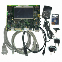
AT91SAM9G45-EKES Atmel, AT91SAM9G45-EKES Datasheet - Page 528

AT91SAM9G45-EKES
Manufacturer Part Number
AT91SAM9G45-EKES
Description
KIT EVAL FOR AT91SAM9G45
Manufacturer
Atmel
Series
AT91SAM Smart ARMr
Type
MCUr
Datasheets
1.AT91SAM9G45-EKES.pdf
(56 pages)
2.AT91SAM9G45-EKES.pdf
(1218 pages)
3.AT91SAM9G45-EKES.pdf
(66 pages)
Specifications of AT91SAM9G45-EKES
Contents
Board
Processor To Be Evaluated
SAM9G45
Data Bus Width
32 bit
Interface Type
I2C, SPI, UART
Maximum Operating Temperature
+ 50 C
Minimum Operating Temperature
- 10 C
Operating Supply Voltage
1.8 V to 3.3 V
For Use With/related Products
AT91SAM9G45
Lead Free Status / RoHS Status
Lead free / RoHS Compliant
Other names
Q4626953
- Current page: 528 of 1218
- Download datasheet (19Mb)
32.5.3
32.6
32.6.1
32.6.2
32.6.3
528
Functional Description
AT91SAM9G45
Interrupt
TC Description
16-bit Counter
Clock Selection
The TC has an interrupt line connected to the Interrupt Controller (IC). Handling the TC interrupt
requires programming the IC before configuring the TC.
The three channels of the Timer Counter are independent and identical in operation . The regis-
ters for channel programming are listed in
Each channel is organized around a 16-bit counter. The value of the counter is incremented at
each positive edge of the selected clock. When the counter has reached the value 0xFFFF and
passes to 0x0000, an overflow occurs and the COVFS bit in TC_SR (Status Register) is set.
The current value of the counter is accessible in real time by reading the Counter Value Regis-
ter, TC_CV. The counter can be reset by a trigger. In this case, the counter value passes to
0x0000 on the next valid edge of the selected clock.
At block level, input clock signals of each channel can either be connected to the external inputs
TCLK0, TCLK1 or TCLK2, or be connected to the internal I/O signals TIOA0, TIOA1 or TIOA2
for chaining by programming the TC_BMR (Block Mode). See
Selection”.
Each channel can independently select an internal or external clock source for its counter:
•
•
This selection is made by the TCCLKS bits in the TC Channel Mode Register.
The selected clock can be inverted with the CLKI bit in TC_CMR. This allows counting on the
opposite edges of the clock.
The burst function allows the clock to be validated when an external signal is high. The BURST
parameter in the Mode Register defines this signal (none, XC0, XC1, XC2). See
”Clock Selection”
Note:
Internal clock signals: TIMER_CLOCK1, TIMER_CLOCK2, TIMER_CLOCK3,
TIMER_CLOCK4, TIMER_CLOCK5
External clock signals: XC0, XC1 or XC2
In all cases, if an external clock is used, the duration of each of its levels must be longer than the
master clock period. The external clock frequency must be at least 2.5 times lower than the mas-
ter clock
Table 32-5 on page
541.
Figure 32-2 ”Clock Chaining
6438F–ATARM–21-Jun-10
Figure 32-3
Related parts for AT91SAM9G45-EKES
Image
Part Number
Description
Manufacturer
Datasheet
Request
R

Part Number:
Description:
MCU ARM9 64K SRAM 144-LFBGA
Manufacturer:
Atmel
Datasheet:

Part Number:
Description:
IC ARM7 MCU FLASH 256K 100LQFP
Manufacturer:
Atmel
Datasheet:

Part Number:
Description:
IC ARM9 MPU 217-LFBGA
Manufacturer:
Atmel
Datasheet:

Part Number:
Description:
MCU ARM9 ULTRA LOW PWR 217-LFBGA
Manufacturer:
Atmel
Datasheet:

Part Number:
Description:
MCU ARM9 324-TFBGA
Manufacturer:
Atmel
Datasheet:

Part Number:
Description:
IC MCU ARM9 SAMPLING 217CBGA
Manufacturer:
Atmel
Datasheet:

Part Number:
Description:
IC ARM9 MCU 217-LFBGA
Manufacturer:
Atmel
Datasheet:

Part Number:
Description:
IC ARM9 MCU 208-PQFP
Manufacturer:
Atmel
Datasheet:

Part Number:
Description:
MCU ARM 512K HS FLASH 100-LQFP
Manufacturer:
Atmel
Datasheet:

Part Number:
Description:
MCU ARM 512K HS FLASH 100-TFBGA
Manufacturer:
Atmel
Datasheet:

Part Number:
Description:
IC ARM9 MCU 200 MHZ 324-TFBGA
Manufacturer:
Atmel
Datasheet:

Part Number:
Description:
IC ARM MCU 16BIT 128K 256BGA
Manufacturer:
Atmel
Datasheet:

Part Number:
Description:
IC ARM7 MCU 32BIT 128K 64LQFP
Manufacturer:
Atmel
Datasheet:

Part Number:
Description:
IC ARM7 MCU FLASH 256K 128-LQFP
Manufacturer:
Atmel
Datasheet:

Part Number:
Description:
IC ARM7 MCU FLASH 512K 128-LQFP
Manufacturer:
Atmel
Datasheet:


