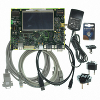
AT91SAM9G45-EKES Atmel, AT91SAM9G45-EKES Datasheet - Page 902

AT91SAM9G45-EKES
Manufacturer Part Number
AT91SAM9G45-EKES
Description
KIT EVAL FOR AT91SAM9G45
Manufacturer
Atmel
Series
AT91SAM Smart ARMr
Type
MCUr
Datasheets
1.AT91SAM9G45-EKES.pdf
(56 pages)
2.AT91SAM9G45-EKES.pdf
(1218 pages)
3.AT91SAM9G45-EKES.pdf
(66 pages)
Specifications of AT91SAM9G45-EKES
Contents
Board
Processor To Be Evaluated
SAM9G45
Data Bus Width
32 bit
Interface Type
I2C, SPI, UART
Maximum Operating Temperature
+ 50 C
Minimum Operating Temperature
- 10 C
Operating Supply Voltage
1.8 V to 3.3 V
For Use With/related Products
AT91SAM9G45
Lead Free Status / RoHS Status
Lead free / RoHS Compliant
Other names
Q4626953
- Current page: 902 of 1218
- Download datasheet (19Mb)
39.4.4.3
39.4.4.4
39.4.4.5
6438F–ATARM–21-Jun-10
Memory Interface
FIFO and DMA Features
Example
Preview datapath contains a data formatter that converts 8:8:8 pixel to RGB 5:6:5 format compli-
ant with 16-bit format of the LCD controller. In general, when converting from a color channel
with more bits to one with fewer bits, formatter module discards the lower-order bits. Example:
Converting from RGB 8:8:8 to RGB 5:6:5, it discards the three LSBs from the red and blue chan-
nels, and two LSBs from the green channel. When grayscale mode is enabled, two memory
formats are supported. One mode supports 2 pixels per word, and the other mode supports 1
pixel per word.
Table 39-8.
Both preview and Codec datapaths contain FIFOs. These asynchronous buffers are used to
safely transfer formatted pixels from Pixel clock domain to AHB clock domain. A video arbiter is
used to manage FIFO thresholds and triggers a relevant DMA request through the AHB master
interface. Thus, depending on FIFO state, a specified length burst is asserted. Regarding AHB
master interface, it supports Scatter DMA mode through linked list operation. This mode of oper-
ation improves flexibility of image buffer location and allows the user to allocate two or more
frame buffers. The destination frame buffers are defined by a series of Frame Buffer Descriptors
(FBD). Each FBD controls the transfer of one entire frame and then optionally loads a further
FBD to switch the DMA operation at another frame buffer address. The FBD is defined by a
series of three words. The first one defines the current frame buffer address (named
DMA_X_ADDR register), the second defines control information (named DMA_X_CTRL regis-
ter) and the third defines the next descriptor address (named DMA_X_DSCR). DMA transfer
mode with linked list support is available for both codec and preview datapath. The data to be
transferred described by an FBD requires several burst accesses. In the example below, the use
of 2 ping-pong frame buffers is described.
The first FBD, stored at address 0x00030000, defines the location of the first frame buffer. This
address is programmed in the ISI user interface DMA_P_DSCR. To enable Descriptor fetch
operation DMA_P_CTRL register must be set to 0x00000001. LLI_0 and LLI_1 are the two
descriptors of the Linked list.
Destination Address: frame buffer ID0 0x02A000 (LLI_0.DMA_P_ADDR)
Transfer 0 Control Information, fetch and writeback: 0x00000003 (LLI_0.DMA_P_CTRL)
Next FBD address: 0x00030010 (LLI_0.DMA_P_DSCR)
Second FBD, stored at address 0x00030010, defines the location of the second frame buffer.
Destination Address: frame buffer ID1 0x0003A000 (LLI_1.DMA_P_ADDR
Transfer 1 Control information fetch and writeback: 0x00000003 (LLI_1.DMA_P_CTRL)
Next FBD address: 0x00030000, wrapping to first FBD (LLI_1.DMA_P_DSCR)
Using this technique, several frame buffers can be configured through the linked list.
illustrates a typical three frame buffer application. Frame n is mapped to frame buffer 0, frame
GS_MODE
0
1
Grayscale Memory Mapping Configuration for 12-bit Data
DATA[31:24]
P_0[11:4]
P_0[11:4]
DATA[23:16]
P_0[3:0], 0000
P_0[3:0], 0000
DATA[15:8]
P_1[11:4]
0
AT91SAM9G45
DATA[7:0]
P_1[3:0], 0000
0
Figure 39-6
902
Related parts for AT91SAM9G45-EKES
Image
Part Number
Description
Manufacturer
Datasheet
Request
R

Part Number:
Description:
MCU ARM9 64K SRAM 144-LFBGA
Manufacturer:
Atmel
Datasheet:

Part Number:
Description:
IC ARM7 MCU FLASH 256K 100LQFP
Manufacturer:
Atmel
Datasheet:

Part Number:
Description:
IC ARM9 MPU 217-LFBGA
Manufacturer:
Atmel
Datasheet:

Part Number:
Description:
MCU ARM9 ULTRA LOW PWR 217-LFBGA
Manufacturer:
Atmel
Datasheet:

Part Number:
Description:
MCU ARM9 324-TFBGA
Manufacturer:
Atmel
Datasheet:

Part Number:
Description:
IC MCU ARM9 SAMPLING 217CBGA
Manufacturer:
Atmel
Datasheet:

Part Number:
Description:
IC ARM9 MCU 217-LFBGA
Manufacturer:
Atmel
Datasheet:

Part Number:
Description:
IC ARM9 MCU 208-PQFP
Manufacturer:
Atmel
Datasheet:

Part Number:
Description:
MCU ARM 512K HS FLASH 100-LQFP
Manufacturer:
Atmel
Datasheet:

Part Number:
Description:
MCU ARM 512K HS FLASH 100-TFBGA
Manufacturer:
Atmel
Datasheet:

Part Number:
Description:
IC ARM9 MCU 200 MHZ 324-TFBGA
Manufacturer:
Atmel
Datasheet:

Part Number:
Description:
IC ARM MCU 16BIT 128K 256BGA
Manufacturer:
Atmel
Datasheet:

Part Number:
Description:
IC ARM7 MCU 32BIT 128K 64LQFP
Manufacturer:
Atmel
Datasheet:

Part Number:
Description:
IC ARM7 MCU FLASH 256K 128-LQFP
Manufacturer:
Atmel
Datasheet:

Part Number:
Description:
IC ARM7 MCU FLASH 512K 128-LQFP
Manufacturer:
Atmel
Datasheet:


