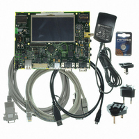
AT91SAM9G45-EKES Atmel, AT91SAM9G45-EKES Datasheet - Page 706

AT91SAM9G45-EKES
Manufacturer Part Number
AT91SAM9G45-EKES
Description
KIT EVAL FOR AT91SAM9G45
Manufacturer
Atmel
Series
AT91SAM Smart ARMr
Type
MCUr
Datasheets
1.AT91SAM9G45-EKES.pdf
(56 pages)
2.AT91SAM9G45-EKES.pdf
(1218 pages)
3.AT91SAM9G45-EKES.pdf
(66 pages)
Specifications of AT91SAM9G45-EKES
Contents
Board
Processor To Be Evaluated
SAM9G45
Data Bus Width
32 bit
Interface Type
I2C, SPI, UART
Maximum Operating Temperature
+ 50 C
Minimum Operating Temperature
- 10 C
Operating Supply Voltage
1.8 V to 3.3 V
For Use With/related Products
AT91SAM9G45
Lead Free Status / RoHS Status
Lead free / RoHS Compliant
Other names
Q4626953
- Current page: 706 of 1218
- Download datasheet (19Mb)
35.4.2.1
35.4.2.2
Table 35-1.
706
Bit
31:2
31
30
29
28
27
1
0
AT91SAM9G45
Address of beginning of buffer
Wrap - marks last descriptor in receive buffer descriptor list.
Ownership - needs to be zero for the EMAC to write data to the receive buffer. The EMAC sets this to one once it has
successfully written a frame to memory.
Software has to clear this bit before the buffer can be used again.
Global all ones broadcast address detected
Multicast hash match
Unicast hash match
External address match
Reserved for future use
FIFO
Receive Buffers
Receive Buffer Descriptor Entry
The FIFO depths are 1
system clock speed, memory latency and network speed.
Data is typically transferred into and out of the FIFOs in bursts of four words. For receive, a bus
request is asserted when the FIFO contains four words and has space for 28 more. For transmit,
a bus request is generated when there is space for four words, or when there is space for 27
words if the next transfer is to be only one or two words.
Thus the bus latency must be less than the time it takes to load the FIFO and transmit or receive
three words (112 bytes) of data.
At 100 Mbit/s, it takes 8960 ns to transmit or receive 112 bytes of data. In addition, six master
clock cycles should be allowed for data to be loaded from the bus and to propagate through the
FIFOs. For a 133 MHz master clock this takes 45 ns, making the bus latency requirement 8915
ns.
Received frames, including CRC/FCS optionally, are written to receive buffers stored in mem-
ory. Each receive buffer is 128 bytes long. The start location for each receive buffer is stored in
memory in a list of receive buffer descriptors at a location pointed to by the receive buffer queue
pointer register. The receive buffer start location is a word address. For the first buffer of a
frame, the start location can be offset by up to three bytes depending on the value written to bits
14 and 15 of the network configuration register. If the start location of the buffer is offset the
available length of the first buffer of a frame is reduced by the corresponding number of bytes.
Each list entry consists of two words, the first being the address of the receive buffer and the
second being the receive status. If the length of a receive frame exceeds the buffer length, the
status word for the used buffer is written with zeroes except for the “start of frame” bit and the
offset bits, if appropriate. Bit zero of the address field is written to one to show the buffer has
been used. The receive buffer manager then reads the location of the next receive buffer and
fills that with receive frame data. The final buffer descriptor status word contains the complete
frame status. Refer to
Table 35-1
28
bytes for receive and 1
Word 0
Word 1
for details of the receive buffer descriptor list.
Function
28
bytes for transmit and are a function of the
6438F–ATARM–21-Jun-10
Related parts for AT91SAM9G45-EKES
Image
Part Number
Description
Manufacturer
Datasheet
Request
R

Part Number:
Description:
MCU ARM9 64K SRAM 144-LFBGA
Manufacturer:
Atmel
Datasheet:

Part Number:
Description:
IC ARM7 MCU FLASH 256K 100LQFP
Manufacturer:
Atmel
Datasheet:

Part Number:
Description:
IC ARM9 MPU 217-LFBGA
Manufacturer:
Atmel
Datasheet:

Part Number:
Description:
MCU ARM9 ULTRA LOW PWR 217-LFBGA
Manufacturer:
Atmel
Datasheet:

Part Number:
Description:
MCU ARM9 324-TFBGA
Manufacturer:
Atmel
Datasheet:

Part Number:
Description:
IC MCU ARM9 SAMPLING 217CBGA
Manufacturer:
Atmel
Datasheet:

Part Number:
Description:
IC ARM9 MCU 217-LFBGA
Manufacturer:
Atmel
Datasheet:

Part Number:
Description:
IC ARM9 MCU 208-PQFP
Manufacturer:
Atmel
Datasheet:

Part Number:
Description:
MCU ARM 512K HS FLASH 100-LQFP
Manufacturer:
Atmel
Datasheet:

Part Number:
Description:
MCU ARM 512K HS FLASH 100-TFBGA
Manufacturer:
Atmel
Datasheet:

Part Number:
Description:
IC ARM9 MCU 200 MHZ 324-TFBGA
Manufacturer:
Atmel
Datasheet:

Part Number:
Description:
IC ARM MCU 16BIT 128K 256BGA
Manufacturer:
Atmel
Datasheet:

Part Number:
Description:
IC ARM7 MCU 32BIT 128K 64LQFP
Manufacturer:
Atmel
Datasheet:

Part Number:
Description:
IC ARM7 MCU FLASH 256K 128-LQFP
Manufacturer:
Atmel
Datasheet:

Part Number:
Description:
IC ARM7 MCU FLASH 512K 128-LQFP
Manufacturer:
Atmel
Datasheet:


