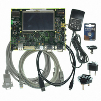
AT91SAM9G45-EKES Atmel, AT91SAM9G45-EKES Datasheet - Page 55

AT91SAM9G45-EKES
Manufacturer Part Number
AT91SAM9G45-EKES
Description
KIT EVAL FOR AT91SAM9G45
Manufacturer
Atmel
Series
AT91SAM Smart ARMr
Type
MCUr
Datasheets
1.AT91SAM9G45-EKES.pdf
(56 pages)
2.AT91SAM9G45-EKES.pdf
(1218 pages)
3.AT91SAM9G45-EKES.pdf
(66 pages)
Specifications of AT91SAM9G45-EKES
Contents
Board
Processor To Be Evaluated
SAM9G45
Data Bus Width
32 bit
Interface Type
I2C, SPI, UART
Maximum Operating Temperature
+ 50 C
Minimum Operating Temperature
- 10 C
Operating Supply Voltage
1.8 V to 3.3 V
For Use With/related Products
AT91SAM9G45
Lead Free Status / RoHS Status
Lead free / RoHS Compliant
Other names
Q4626953
- Current page: 55 of 1218
- Download datasheet (19Mb)
10.6
10.6.1
10.6.2
10.6.3
6438F–ATARM–21-Jun-10
Functional Description
Test Pin
EmbeddedICE
JTAG Signal Description
One dedicated pin, TST, is used to define the device operating mode. The user must make sure
that this pin is tied at low level to ensure normal operating conditions. Other values associated
with this pin are reserved for manufacturing test.
The ARM9EJ-S EmbeddedICE-RT
host computer via an ICE interface. Debug support is implemented using an ARM9EJ-S core
embedded within the ARM926EJ-S. The internal state of the ARM926EJ-S is examined through
an ICE/JTAG port which allows instructions to be serially inserted into the pipeline of the core
without using the external data bus. Therefore, when in debug state, a store-multiple (STM) can
be inserted into the instruction pipeline. This exports the contents of the ARM9EJ-S registers.
This data can be serially shifted out without affecting the rest of the system.
There are two scan chains inside the ARM9EJ-S processor which support testing, debugging,
and programming of the EmbeddedICE-RT. The scan chains are controlled by the ICE/JTAG
port.
EmbeddedICE mode is selected when JTAGSEL is low. It is not possible to switch directly
between ICE and JTAG operations. A chip reset must be performed after JTAGSEL is changed.
For further details on the EmbeddedICE-RT, see the ARM document:
ARM9EJ-S Technical Reference Manual (DDI 0222A).
TMS is the Test Mode Select input which controls the transitions of the test interface state
machine.
TDI is the Test Data Input line which supplies the data to the JTAG registers (Boundary Scan
Register, Instruction Register, or other data registers).
TDO is the Test Data Output line which is used to serially output the data from the JTAG regis-
ters to the equipment controlling the test. It carries the sampled values from the boundary scan
chain (or other JTAG registers) and propagates them to the next chip in the serial test circuit.
NTRST (optional in IEEE Standard 1149.1) is a Test-ReSeT input which is mandatory in ARM
cores and used to reset the debug logic. On Atmel ARM926EJ-S-based cores, NTRST is a
Power On Reset output. It is asserted on power on. If necessary, the user can also reset the
debug logic with the NTRST pin assertion during 2.5 MCK periods.
TCK is the Test ClocK input which enables the test interface. TCK is pulsed by the equipment
controlling the test and not by the tested device. It can be pulsed at any frequency. Note the
maximum JTAG clock rate on ARM926EJ-S cores is 1/6th the clock of the CPU. This gives 5.45
kHz maximum initial JTAG clock rate for an ARM9E running from the 32.768 kHz slow clock.
RTCK is the Return Test Clock. Not an IEEE Standard 1149.1 signal added for a better clock
handling by emulators. From some ICE Interface probes, this return signal can be used to syn-
chronize the TCK clock and take not care about the given ratio between the ICE Interface clock
and system clock equal to 1/6th. This signal is only available in JTAG ICE Mode and not in
boundary scan mode.
™
is supported via the ICE/JTAG port. It is connected to a
AT91SAM9G45
55
Related parts for AT91SAM9G45-EKES
Image
Part Number
Description
Manufacturer
Datasheet
Request
R

Part Number:
Description:
MCU ARM9 64K SRAM 144-LFBGA
Manufacturer:
Atmel
Datasheet:

Part Number:
Description:
IC ARM7 MCU FLASH 256K 100LQFP
Manufacturer:
Atmel
Datasheet:

Part Number:
Description:
IC ARM9 MPU 217-LFBGA
Manufacturer:
Atmel
Datasheet:

Part Number:
Description:
MCU ARM9 ULTRA LOW PWR 217-LFBGA
Manufacturer:
Atmel
Datasheet:

Part Number:
Description:
MCU ARM9 324-TFBGA
Manufacturer:
Atmel
Datasheet:

Part Number:
Description:
IC MCU ARM9 SAMPLING 217CBGA
Manufacturer:
Atmel
Datasheet:

Part Number:
Description:
IC ARM9 MCU 217-LFBGA
Manufacturer:
Atmel
Datasheet:

Part Number:
Description:
IC ARM9 MCU 208-PQFP
Manufacturer:
Atmel
Datasheet:

Part Number:
Description:
MCU ARM 512K HS FLASH 100-LQFP
Manufacturer:
Atmel
Datasheet:

Part Number:
Description:
MCU ARM 512K HS FLASH 100-TFBGA
Manufacturer:
Atmel
Datasheet:

Part Number:
Description:
IC ARM9 MCU 200 MHZ 324-TFBGA
Manufacturer:
Atmel
Datasheet:

Part Number:
Description:
IC ARM MCU 16BIT 128K 256BGA
Manufacturer:
Atmel
Datasheet:

Part Number:
Description:
IC ARM7 MCU 32BIT 128K 64LQFP
Manufacturer:
Atmel
Datasheet:

Part Number:
Description:
IC ARM7 MCU FLASH 256K 128-LQFP
Manufacturer:
Atmel
Datasheet:

Part Number:
Description:
IC ARM7 MCU FLASH 512K 128-LQFP
Manufacturer:
Atmel
Datasheet:


