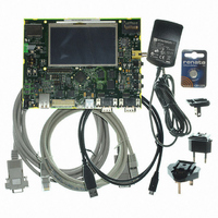
AT91SAM9G45-EKES Atmel, AT91SAM9G45-EKES Datasheet - Page 459

AT91SAM9G45-EKES
Manufacturer Part Number
AT91SAM9G45-EKES
Description
KIT EVAL FOR AT91SAM9G45
Manufacturer
Atmel
Series
AT91SAM Smart ARMr
Type
MCUr
Datasheets
1.AT91SAM9G45-EKES.pdf
(56 pages)
2.AT91SAM9G45-EKES.pdf
(1218 pages)
3.AT91SAM9G45-EKES.pdf
(66 pages)
Specifications of AT91SAM9G45-EKES
Contents
Board
Processor To Be Evaluated
SAM9G45
Data Bus Width
32 bit
Interface Type
I2C, SPI, UART
Maximum Operating Temperature
+ 50 C
Minimum Operating Temperature
- 10 C
Operating Supply Voltage
1.8 V to 3.3 V
For Use With/related Products
AT91SAM9G45
Lead Free Status / RoHS Status
Lead free / RoHS Compliant
Other names
Q4626953
- Current page: 459 of 1218
- Download datasheet (19Mb)
Figure 30-4. Output Line Timings
30.4.8
30.4.9
6438F–ATARM–21-Jun-10
Write PIO_ODSR at 1
Write PIO_ODSR at 0
Write PIO_CODR
Write PIO_SODR
Inputs
Input Glitch Filtering
PIO_ODSR
PIO_PDSR
MCK
The level on each I/O line can be read through PIO_PDSR (Pin Data Status Register). This reg-
ister indicates the level of the I/O lines regardless of their configuration, whether uniquely as an
input or driven by the PIO controller or driven by a peripheral.
Reading the I/O line levels requires the clock of the PIO controller to be enabled, otherwise
PIO_PDSR reads the levels present on the I/O line at the time the clock was disabled.
Optional input glitch filters are independently programmable on each I/O line. When the glitch fil-
ter is enabled, a glitch with a duration of less than 1/2 Master Clock (MCK) cycle is automatically
rejected, while a pulse with a duration of 1 Master Clock cycle or more is accepted. For pulse
durations between 1/2 Master Clock cycle and 1 Master Clock cycle the pulse may or may not
be taken into account, depending on the precise timing of its occurrence. Thus for a pulse to be
visible it must exceed 1 Master Clock cycle, whereas for a glitch to be reliably filtered out, its
duration must not exceed 1/2 Master Clock cycle. The filter introduces one Master Clock cycle
latency if the pin level change occurs before a rising edge. However, this latency does not
appear if the pin level change occurs before a falling edge. This is illustrated in
The glitch filters are controlled by the register set; PIO_IFER (Input Filter Enable Register),
PIO_IFDR (Input Filter Disable Register) and PIO_IFSR (Input Filter Status Register). Writing
PIO_IFER and PIO_IFDR respectively sets and clears bits in PIO_IFSR. This last register
enables the glitch filter on the I/O lines.
When the glitch filter is enabled, it does not modify the behavior of the inputs on the peripherals.
It acts only on the value read in PIO_PDSR and on the input change interrupt detection. The
glitch filters require that the PIO Controller clock is enabled.
APB Access
2 cycles
APB Access
AT91SAM9G45
2 cycles
Figure
30-5.
459
Related parts for AT91SAM9G45-EKES
Image
Part Number
Description
Manufacturer
Datasheet
Request
R

Part Number:
Description:
MCU ARM9 64K SRAM 144-LFBGA
Manufacturer:
Atmel
Datasheet:

Part Number:
Description:
IC ARM7 MCU FLASH 256K 100LQFP
Manufacturer:
Atmel
Datasheet:

Part Number:
Description:
IC ARM9 MPU 217-LFBGA
Manufacturer:
Atmel
Datasheet:

Part Number:
Description:
MCU ARM9 ULTRA LOW PWR 217-LFBGA
Manufacturer:
Atmel
Datasheet:

Part Number:
Description:
MCU ARM9 324-TFBGA
Manufacturer:
Atmel
Datasheet:

Part Number:
Description:
IC MCU ARM9 SAMPLING 217CBGA
Manufacturer:
Atmel
Datasheet:

Part Number:
Description:
IC ARM9 MCU 217-LFBGA
Manufacturer:
Atmel
Datasheet:

Part Number:
Description:
IC ARM9 MCU 208-PQFP
Manufacturer:
Atmel
Datasheet:

Part Number:
Description:
MCU ARM 512K HS FLASH 100-LQFP
Manufacturer:
Atmel
Datasheet:

Part Number:
Description:
MCU ARM 512K HS FLASH 100-TFBGA
Manufacturer:
Atmel
Datasheet:

Part Number:
Description:
IC ARM9 MCU 200 MHZ 324-TFBGA
Manufacturer:
Atmel
Datasheet:

Part Number:
Description:
IC ARM MCU 16BIT 128K 256BGA
Manufacturer:
Atmel
Datasheet:

Part Number:
Description:
IC ARM7 MCU 32BIT 128K 64LQFP
Manufacturer:
Atmel
Datasheet:

Part Number:
Description:
IC ARM7 MCU FLASH 256K 128-LQFP
Manufacturer:
Atmel
Datasheet:

Part Number:
Description:
IC ARM7 MCU FLASH 512K 128-LQFP
Manufacturer:
Atmel
Datasheet:


