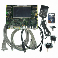
AT91SAM9G45-EKES Atmel, AT91SAM9G45-EKES Datasheet - Page 183

AT91SAM9G45-EKES
Manufacturer Part Number
AT91SAM9G45-EKES
Description
KIT EVAL FOR AT91SAM9G45
Manufacturer
Atmel
Series
AT91SAM Smart ARMr
Type
MCUr
Datasheets
1.AT91SAM9G45-EKES.pdf
(56 pages)
2.AT91SAM9G45-EKES.pdf
(1218 pages)
3.AT91SAM9G45-EKES.pdf
(66 pages)
Specifications of AT91SAM9G45-EKES
Contents
Board
Processor To Be Evaluated
SAM9G45
Data Bus Width
32 bit
Interface Type
I2C, SPI, UART
Maximum Operating Temperature
+ 50 C
Minimum Operating Temperature
- 10 C
Operating Supply Voltage
1.8 V to 3.3 V
For Use With/related Products
AT91SAM9G45
Lead Free Status / RoHS Status
Lead free / RoHS Compliant
Other names
Q4626953
- Current page: 183 of 1218
- Download datasheet (19Mb)
20.2.9
6438F–ATARM–21-Jun-10
Programmable I/O Lines Power Supplies and Drive Levels
The power supply pin VDDIOM1 accepts two voltage ranges. This allows the device to reach its
maximum speed either out of 1.8V or 3.3V external memories.
The maximum speed is 133 MHz on the SDCK pin and #SDCK signals loaded with 10 pF. The
load on data/address and control signals are 30 pF for power supply at 1.8V and 50 pF for power
supply at 3.3V. The data lines frequency reaches 133 MHz in DDR2 mode. The other signals
(control and address) do not go over 66 MHz.
The EBI I/Os accept two drive levels, HIGH and LOW. This allows to avoid overshoots and give
the best performance according to the bus load and external memories. Refer to the EBI Chip
Select Assignment Register for more details.
The voltage ranges and the drive level are determined by programming EBI_DRIVE field in the
Chip Configuration registers located in the Matrix User Interface.
At reset the selected default drive level is High.
At reset, the selected voltage defaults to 3.3V typical and power supply pins can accept either
1.8V or 3.3V. The user must make sure to program the EBI voltage range before getting the
device out of its Slow Clock Mode. The user must make sure to program the EBI voltage range
before getting the device out of its Slow Clock Mode.
• Assign the EBI CS4 and/or EBI_CS5 to the CompactFlash Slot 0 and/or Slot 1 by setting the
• The address line A21 is to select Alternate True IDE (A21=1) or True IDE (A21=0) modes.
• A21, CFRNW, CFS0, CFCS1, CFCE1 and CFCE2 signals are multiplexed with PIO lines and
• Configure a PIO line as an output for CFRST and two others as an input for CFIRQ and
• Configure SMC CS4 and/or SMC_CS5 (for Slot 0 or 1) Setup, Pulse, Cycle and Mode
bit EBI_CS4A and/or EBI_CS5A in the EBI Chip Select Assignment Register located in the
bus matrix memory space.
thus the dedicated PIOs must be programmed in peripheral mode in the PIO controller.
CARD DETECT functions respectively.
accordingly to CompactFlash timings and system bus frequency.
AT91SAM9G45
183
Related parts for AT91SAM9G45-EKES
Image
Part Number
Description
Manufacturer
Datasheet
Request
R

Part Number:
Description:
MCU ARM9 64K SRAM 144-LFBGA
Manufacturer:
Atmel
Datasheet:

Part Number:
Description:
IC ARM7 MCU FLASH 256K 100LQFP
Manufacturer:
Atmel
Datasheet:

Part Number:
Description:
IC ARM9 MPU 217-LFBGA
Manufacturer:
Atmel
Datasheet:

Part Number:
Description:
MCU ARM9 ULTRA LOW PWR 217-LFBGA
Manufacturer:
Atmel
Datasheet:

Part Number:
Description:
MCU ARM9 324-TFBGA
Manufacturer:
Atmel
Datasheet:

Part Number:
Description:
IC MCU ARM9 SAMPLING 217CBGA
Manufacturer:
Atmel
Datasheet:

Part Number:
Description:
IC ARM9 MCU 217-LFBGA
Manufacturer:
Atmel
Datasheet:

Part Number:
Description:
IC ARM9 MCU 208-PQFP
Manufacturer:
Atmel
Datasheet:

Part Number:
Description:
MCU ARM 512K HS FLASH 100-LQFP
Manufacturer:
Atmel
Datasheet:

Part Number:
Description:
MCU ARM 512K HS FLASH 100-TFBGA
Manufacturer:
Atmel
Datasheet:

Part Number:
Description:
IC ARM9 MCU 200 MHZ 324-TFBGA
Manufacturer:
Atmel
Datasheet:

Part Number:
Description:
IC ARM MCU 16BIT 128K 256BGA
Manufacturer:
Atmel
Datasheet:

Part Number:
Description:
IC ARM7 MCU 32BIT 128K 64LQFP
Manufacturer:
Atmel
Datasheet:

Part Number:
Description:
IC ARM7 MCU FLASH 256K 128-LQFP
Manufacturer:
Atmel
Datasheet:

Part Number:
Description:
IC ARM7 MCU FLASH 512K 128-LQFP
Manufacturer:
Atmel
Datasheet:


