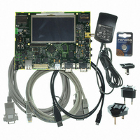
AT91SAM9G45-EKES Atmel, AT91SAM9G45-EKES Datasheet - Page 298

AT91SAM9G45-EKES
Manufacturer Part Number
AT91SAM9G45-EKES
Description
KIT EVAL FOR AT91SAM9G45
Manufacturer
Atmel
Series
AT91SAM Smart ARMr
Type
MCUr
Datasheets
1.AT91SAM9G45-EKES.pdf
(56 pages)
2.AT91SAM9G45-EKES.pdf
(1218 pages)
3.AT91SAM9G45-EKES.pdf
(66 pages)
Specifications of AT91SAM9G45-EKES
Contents
Board
Processor To Be Evaluated
SAM9G45
Data Bus Width
32 bit
Interface Type
I2C, SPI, UART
Maximum Operating Temperature
+ 50 C
Minimum Operating Temperature
- 10 C
Operating Supply Voltage
1.8 V to 3.3 V
For Use With/related Products
AT91SAM9G45
Lead Free Status / RoHS Status
Lead free / RoHS Compliant
Other names
Q4626953
- Current page: 298 of 1218
- Download datasheet (19Mb)
24.6.4
24.7
24.7.1
298
Divider and PLLA Block
AT91SAM9G45
Main Oscillator Bypass
Divider and Phase Lock Loop Programming
When the MOSCEN bit and the OSCOUNT are written in CKGR_MOR to enable the main oscil-
lator, the MOSCS bit in PMC_SR (Status Register) is cleared and the counter starts counting
down on the slow clock divided by 8 from the OSCOUNT value. Since the OSCOUNT value is
coded with 8 bits, the maximum startup time is about 62 ms.
When the counter reaches 0, the MOSCS bit is set, indicating that the main clock is valid. Set-
ting the MOSCS bit in PMC_IMR can trigger an interrupt to the processor.
The user can input a clock on the device instead of connecting a crystal. In this case, the user
has to provide the external clock signal on the XIN pin. The input characteristics of the XIN pin
under these conditions are given in the product electrical characteristics section. The program-
mer has to be sure to set the OSCBYPASS bit to 1 and the MOSCEN bit to 0 in the Main OSC
register (CKGR_MOR) for the external clock to operate properly.
The PLLA embeds an input divider to increase the accuracy of the resulting clock signals. How-
ever, the user must respect the PLLA minimum input frequency when programming the divider.
The PLLA embeds also an output divisor by 2.
Figure 24-6
Figure 24-6. Divider and PLLA Block Diagram
The divider can be set between 1 and 255 in steps of 1. When a divider field (DIV) is set to 0, the
output of the corresponding divider and the PLL output is a continuous signal at level 0. On
reset, each DIV field is set to 0, thus the corresponding PLL input clock is set to 0.
The PLLA allows multiplication of the divider’s outputs. The PLLA clock signal has a frequency
that depends on the respective source signal frequency and on the parameters DIVA and
MULA. The factor applied to the source signal frequency is (MULA + 1)/DIVA. When MULA is
written to 0, the PLLA is disabled and its power consumption is saved. Re-enabling the PLLA
can be performed by writing a value higher than 0 in the MUL field.
Whenever the PLLA is re-enabled or one of its parameters is changed, the LOCKA bit in
PMC_SR is automatically cleared. The values written in the PLLACOUNT field in CKGR_PLLAR
are loaded in the PLLA counter. The PLLA counter then decrements at the speed of the Slow
MAINCK
shows the block diagram of the divider and PLLA block.
SLCK
Divider
DIVA
PLLACOUNT
Counter
PLLA
MULA
PLLA
OUTA
LOCKA
PLLADIV2
/1 or /2
Divider
6438F–ATARM–21-Jun-10
PLLACK
Related parts for AT91SAM9G45-EKES
Image
Part Number
Description
Manufacturer
Datasheet
Request
R

Part Number:
Description:
MCU ARM9 64K SRAM 144-LFBGA
Manufacturer:
Atmel
Datasheet:

Part Number:
Description:
IC ARM7 MCU FLASH 256K 100LQFP
Manufacturer:
Atmel
Datasheet:

Part Number:
Description:
IC ARM9 MPU 217-LFBGA
Manufacturer:
Atmel
Datasheet:

Part Number:
Description:
MCU ARM9 ULTRA LOW PWR 217-LFBGA
Manufacturer:
Atmel
Datasheet:

Part Number:
Description:
MCU ARM9 324-TFBGA
Manufacturer:
Atmel
Datasheet:

Part Number:
Description:
IC MCU ARM9 SAMPLING 217CBGA
Manufacturer:
Atmel
Datasheet:

Part Number:
Description:
IC ARM9 MCU 217-LFBGA
Manufacturer:
Atmel
Datasheet:

Part Number:
Description:
IC ARM9 MCU 208-PQFP
Manufacturer:
Atmel
Datasheet:

Part Number:
Description:
MCU ARM 512K HS FLASH 100-LQFP
Manufacturer:
Atmel
Datasheet:

Part Number:
Description:
MCU ARM 512K HS FLASH 100-TFBGA
Manufacturer:
Atmel
Datasheet:

Part Number:
Description:
IC ARM9 MCU 200 MHZ 324-TFBGA
Manufacturer:
Atmel
Datasheet:

Part Number:
Description:
IC ARM MCU 16BIT 128K 256BGA
Manufacturer:
Atmel
Datasheet:

Part Number:
Description:
IC ARM7 MCU 32BIT 128K 64LQFP
Manufacturer:
Atmel
Datasheet:

Part Number:
Description:
IC ARM7 MCU FLASH 256K 128-LQFP
Manufacturer:
Atmel
Datasheet:

Part Number:
Description:
IC ARM7 MCU FLASH 512K 128-LQFP
Manufacturer:
Atmel
Datasheet:


