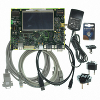
AT91SAM9G45-EKES Atmel, AT91SAM9G45-EKES Datasheet - Page 199

AT91SAM9G45-EKES
Manufacturer Part Number
AT91SAM9G45-EKES
Description
KIT EVAL FOR AT91SAM9G45
Manufacturer
Atmel
Series
AT91SAM Smart ARMr
Type
MCUr
Datasheets
1.AT91SAM9G45-EKES.pdf
(56 pages)
2.AT91SAM9G45-EKES.pdf
(1218 pages)
3.AT91SAM9G45-EKES.pdf
(66 pages)
Specifications of AT91SAM9G45-EKES
Contents
Board
Processor To Be Evaluated
SAM9G45
Data Bus Width
32 bit
Interface Type
I2C, SPI, UART
Maximum Operating Temperature
+ 50 C
Minimum Operating Temperature
- 10 C
Operating Supply Voltage
1.8 V to 3.3 V
For Use With/related Products
AT91SAM9G45
Lead Free Status / RoHS Status
Lead free / RoHS Compliant
Other names
Q4626953
- Current page: 199 of 1218
- Download datasheet (19Mb)
Figure 21-15. WRITE_MODE = 0. The write operation is controlled by NCS
21.8.5
Table 21-4.
21.8.6
6438F–ATARM–21-Jun-10
Coded Value
setup [5:0]
pulse [6:0]
cycle [8:0]
Coding Timing Parameters
Reset Values of Timing Parameters
Coding and Range of Timing Parameters
NWR0, NWR1,
NWR2, NWR3
NBS0, NBS1,
NBS2, NBS3,
A0, A1
Number of Bits
D[31:0]
A
NWE,
[25:2]
MCK
All timing parameters are defined for one chip select and are grouped together in one
SMC_REGISTER according to their type.
The SMC_SETUP register groups the definition of all setup parameters:
• NRD_SETUP, NCS_RD_SETUP, NWE_SETUP, NCS_WR_SETUP
The SMC_PULSE register groups the definition of all pulse parameters:
• NRD_PULSE, NCS_RD_PULSE, NWE_PULSE, NCS_WR_PULSE
The SMC_CYCLE register groups the definition of all cycle parameters:
• NRD_CYCLE, NWE_CYCLE
Table 21-4
Table 21-8
NCS
6
7
9
shows how the timing parameters are coded and their permitted range.
gives the default value of timing parameters at reset.
256 x cycle[8:7] + cycle[6:0]
128 x setup[5] + setup[4:0]
256 x pulse[6] + pulse[5:0]
Effective Value
Coded Value
0
0
0
127
31
63
Permitted Range
AT91SAM9G45
Effective Value
0
0
0
0
0
256+127
512+127
768+127
128+31
256+63
199
Related parts for AT91SAM9G45-EKES
Image
Part Number
Description
Manufacturer
Datasheet
Request
R

Part Number:
Description:
MCU ARM9 64K SRAM 144-LFBGA
Manufacturer:
Atmel
Datasheet:

Part Number:
Description:
IC ARM7 MCU FLASH 256K 100LQFP
Manufacturer:
Atmel
Datasheet:

Part Number:
Description:
IC ARM9 MPU 217-LFBGA
Manufacturer:
Atmel
Datasheet:

Part Number:
Description:
MCU ARM9 ULTRA LOW PWR 217-LFBGA
Manufacturer:
Atmel
Datasheet:

Part Number:
Description:
MCU ARM9 324-TFBGA
Manufacturer:
Atmel
Datasheet:

Part Number:
Description:
IC MCU ARM9 SAMPLING 217CBGA
Manufacturer:
Atmel
Datasheet:

Part Number:
Description:
IC ARM9 MCU 217-LFBGA
Manufacturer:
Atmel
Datasheet:

Part Number:
Description:
IC ARM9 MCU 208-PQFP
Manufacturer:
Atmel
Datasheet:

Part Number:
Description:
MCU ARM 512K HS FLASH 100-LQFP
Manufacturer:
Atmel
Datasheet:

Part Number:
Description:
MCU ARM 512K HS FLASH 100-TFBGA
Manufacturer:
Atmel
Datasheet:

Part Number:
Description:
IC ARM9 MCU 200 MHZ 324-TFBGA
Manufacturer:
Atmel
Datasheet:

Part Number:
Description:
IC ARM MCU 16BIT 128K 256BGA
Manufacturer:
Atmel
Datasheet:

Part Number:
Description:
IC ARM7 MCU 32BIT 128K 64LQFP
Manufacturer:
Atmel
Datasheet:

Part Number:
Description:
IC ARM7 MCU FLASH 256K 128-LQFP
Manufacturer:
Atmel
Datasheet:

Part Number:
Description:
IC ARM7 MCU FLASH 512K 128-LQFP
Manufacturer:
Atmel
Datasheet:


