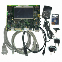
AT91SAM9G45-EKES Atmel, AT91SAM9G45-EKES Datasheet - Page 200

AT91SAM9G45-EKES
Manufacturer Part Number
AT91SAM9G45-EKES
Description
KIT EVAL FOR AT91SAM9G45
Manufacturer
Atmel
Series
AT91SAM Smart ARMr
Type
MCUr
Datasheets
1.AT91SAM9G45-EKES.pdf
(56 pages)
2.AT91SAM9G45-EKES.pdf
(1218 pages)
3.AT91SAM9G45-EKES.pdf
(66 pages)
Specifications of AT91SAM9G45-EKES
Contents
Board
Processor To Be Evaluated
SAM9G45
Data Bus Width
32 bit
Interface Type
I2C, SPI, UART
Maximum Operating Temperature
+ 50 C
Minimum Operating Temperature
- 10 C
Operating Supply Voltage
1.8 V to 3.3 V
For Use With/related Products
AT91SAM9G45
Lead Free Status / RoHS Status
Lead free / RoHS Compliant
Other names
Q4626953
- Current page: 200 of 1218
- Download datasheet (19Mb)
21.8.7
21.9
21.9.1
200
Automatic Wait States
AT91SAM9G45
Usage Restriction
Chip Select Wait States
The SMC does not check the validity of the user-programmed parameters. If the sum of SETUP
and PULSE parameters is larger than the corresponding CYCLE parameter, this leads to unpre-
dictable behavior of the SMC.
For read operations:
Null but positive setup and hold of address and NRD and/or NCS can not be guaranteed at the
memory interface because of the propagation delay of theses signals through external logic and
pads. If positive setup and hold values must be verified, then it is strictly recommended to pro-
gram non-null values so as to cover possible skews between address, NCS and NRD signals.
For write operations:
If a null hold value is programmed on NWE, the SMC can guarantee a positive hold of address,
byte select lines, and NCS signal after the rising edge of NWE. This is true for WRITE_MODE =
1 only. See
For read and write operations: a null value for pulse parameters is forbidden and may lead to
unpredictable behavior.
In read and write cycles, the setup and hold time parameters are defined in reference to the
address bus. For external devices that require setup and hold time between NCS and NRD sig-
nals (read), or between NCS and NWE signals (write), these setup and hold times must be
converted into setup and hold times in reference to the address bus.
Under certain circumstances, the SMC automatically inserts idle cycles between accesses to
avoid bus contention or operation conflict.
The SMC always inserts an idle cycle between 2 transfers on separate chip selects. This idle
cycle ensures that there is no bus contention between the de-activation of one device and the
activation of the next one.
During chip select wait state, all control lines are turned inactive: NBS0 to NBS3, NWR0 to
NWR3, NCS[0..5], NRD lines are all set to 1.
Figure 21-16
Select 2.
“Early Read Wait State” on page
illustrates a chip select wait state between access on Chip Select 0 and Chip
201.
6438F–ATARM–21-Jun-10
Related parts for AT91SAM9G45-EKES
Image
Part Number
Description
Manufacturer
Datasheet
Request
R

Part Number:
Description:
MCU ARM9 64K SRAM 144-LFBGA
Manufacturer:
Atmel
Datasheet:

Part Number:
Description:
IC ARM7 MCU FLASH 256K 100LQFP
Manufacturer:
Atmel
Datasheet:

Part Number:
Description:
IC ARM9 MPU 217-LFBGA
Manufacturer:
Atmel
Datasheet:

Part Number:
Description:
MCU ARM9 ULTRA LOW PWR 217-LFBGA
Manufacturer:
Atmel
Datasheet:

Part Number:
Description:
MCU ARM9 324-TFBGA
Manufacturer:
Atmel
Datasheet:

Part Number:
Description:
IC MCU ARM9 SAMPLING 217CBGA
Manufacturer:
Atmel
Datasheet:

Part Number:
Description:
IC ARM9 MCU 217-LFBGA
Manufacturer:
Atmel
Datasheet:

Part Number:
Description:
IC ARM9 MCU 208-PQFP
Manufacturer:
Atmel
Datasheet:

Part Number:
Description:
MCU ARM 512K HS FLASH 100-LQFP
Manufacturer:
Atmel
Datasheet:

Part Number:
Description:
MCU ARM 512K HS FLASH 100-TFBGA
Manufacturer:
Atmel
Datasheet:

Part Number:
Description:
IC ARM9 MCU 200 MHZ 324-TFBGA
Manufacturer:
Atmel
Datasheet:

Part Number:
Description:
IC ARM MCU 16BIT 128K 256BGA
Manufacturer:
Atmel
Datasheet:

Part Number:
Description:
IC ARM7 MCU 32BIT 128K 64LQFP
Manufacturer:
Atmel
Datasheet:

Part Number:
Description:
IC ARM7 MCU FLASH 256K 128-LQFP
Manufacturer:
Atmel
Datasheet:

Part Number:
Description:
IC ARM7 MCU FLASH 512K 128-LQFP
Manufacturer:
Atmel
Datasheet:


