AT91SAM9G45-EKES Atmel, AT91SAM9G45-EKES Datasheet - Page 427

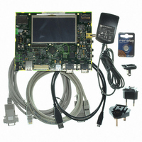
AT91SAM9G45-EKES
Manufacturer Part Number
AT91SAM9G45-EKES
Description
KIT EVAL FOR AT91SAM9G45
Manufacturer
Atmel
Series
AT91SAM Smart ARMr
Type
MCUr
Datasheets
1.AT91SAM9G45-EKES.pdf
(56 pages)
2.AT91SAM9G45-EKES.pdf
(1218 pages)
3.AT91SAM9G45-EKES.pdf
(66 pages)
Specifications of AT91SAM9G45-EKES
Contents
Board
Processor To Be Evaluated
SAM9G45
Data Bus Width
32 bit
Interface Type
I2C, SPI, UART
Maximum Operating Temperature
+ 50 C
Minimum Operating Temperature
- 10 C
Operating Supply Voltage
1.8 V to 3.3 V
For Use With/related Products
AT91SAM9G45
Lead Free Status / RoHS Status
Lead free / RoHS Compliant
Other names
Q4626953
- Current page: 427 of 1218
- Download datasheet (19Mb)
Figure 29-5. SPI Transfer Format (NCPHA = 0, 8 bits per transfer)
29.7.3
6438F–ATARM–21-Jun-10
SPCK cycle (for reference)
(from master)
(from slave)
(CPOL = 0)
(CPOL = 1)
(to slave)
Master Mode Operations
SPCK
SPCK
MOSI
MISO
NSS
*
When configured in Master Mode, the SPI operates on the clock generated by the internal pro-
grammable baud rate generator. It fully controls the data transfers to and from the slave(s)
connected to the SPI bus. The SPI drives the chip select line to the slave and the serial clock
signal (SPCK).
The SPI features two holding registers, the Transmit Data Register and the Receive Data Regis-
ter, and a single Shift Register. The holding registers maintain the data flow at a constant rate.
After enabling the SPI, a data transfer begins when the processor writes to the SPI_TDR (Trans-
mit Data Register). The written data is immediately transferred in the Shift Register and transfer
on the SPI bus starts. While the data in the Shift Register is shifted on the MOSI line, the MISO
line is sampled and shifted in the Shift Register. Receiving data cannot occur without transmit-
ting data. If receiving mode is not needed, for example when communicating with a slave
receiver only (such as an LCD), the receive status flags in the status register can be discarded.
Before writing the TDR, the PCS field in the SPI_MR register must be set in order to select a
slave.
After enabling the SPI, a data transfer begins when the processor writes to the SPI_TDR (Trans-
mit Data Register). The written data is immediately transferred in the Shift Register and transfer
on the SPI bus starts. While the data in the Shift Register is shifted on the MOSI line, the MISO
line is sampled and shifted in the Shift Register. Transmission cannot occur without reception.
Before writing the TDR, the PCS field must be set in order to select a slave.
If new data is written in SPI_TDR during the transfer, it stays in it until the current transfer is
completed. Then, the received data is transferred from the Shift Register to SPI_RDR, the data
in SPI_TDR is loaded in the Shift Register and a new transfer starts.
* Not defined but normally LSB of previous character transmitted.
1
MSB
MSB
2
6
6
3
5
5
4
4
4
5
3
3
6
2
2
7
1
1
AT91SAM9G45
8
LSB
LSB
427
Related parts for AT91SAM9G45-EKES
Image
Part Number
Description
Manufacturer
Datasheet
Request
R

Part Number:
Description:
MCU ARM9 64K SRAM 144-LFBGA
Manufacturer:
Atmel
Datasheet:

Part Number:
Description:
IC ARM7 MCU FLASH 256K 100LQFP
Manufacturer:
Atmel
Datasheet:

Part Number:
Description:
IC ARM9 MPU 217-LFBGA
Manufacturer:
Atmel
Datasheet:

Part Number:
Description:
MCU ARM9 ULTRA LOW PWR 217-LFBGA
Manufacturer:
Atmel
Datasheet:

Part Number:
Description:
MCU ARM9 324-TFBGA
Manufacturer:
Atmel
Datasheet:

Part Number:
Description:
IC MCU ARM9 SAMPLING 217CBGA
Manufacturer:
Atmel
Datasheet:

Part Number:
Description:
IC ARM9 MCU 217-LFBGA
Manufacturer:
Atmel
Datasheet:

Part Number:
Description:
IC ARM9 MCU 208-PQFP
Manufacturer:
Atmel
Datasheet:

Part Number:
Description:
MCU ARM 512K HS FLASH 100-LQFP
Manufacturer:
Atmel
Datasheet:

Part Number:
Description:
MCU ARM 512K HS FLASH 100-TFBGA
Manufacturer:
Atmel
Datasheet:

Part Number:
Description:
IC ARM9 MCU 200 MHZ 324-TFBGA
Manufacturer:
Atmel
Datasheet:

Part Number:
Description:
IC ARM MCU 16BIT 128K 256BGA
Manufacturer:
Atmel
Datasheet:

Part Number:
Description:
IC ARM7 MCU 32BIT 128K 64LQFP
Manufacturer:
Atmel
Datasheet:

Part Number:
Description:
IC ARM7 MCU FLASH 256K 128-LQFP
Manufacturer:
Atmel
Datasheet:

Part Number:
Description:
IC ARM7 MCU FLASH 512K 128-LQFP
Manufacturer:
Atmel
Datasheet:


