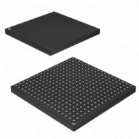
AT91SAM9G45-CU Atmel, AT91SAM9G45-CU Datasheet - Page 1035

AT91SAM9G45-CU
Manufacturer Part Number
AT91SAM9G45-CU
Description
MCU ARM9 324-TFBGA
Manufacturer
Atmel
Series
AT91SAMr
Datasheets
1.AT91SAM9G45-EKES.pdf
(56 pages)
2.AT91SAM9G45-EKES.pdf
(1218 pages)
3.AT91SAM9G45-CU.pdf
(10 pages)
Specifications of AT91SAM9G45-CU
Core Processor
ARM9
Core Size
16/32-Bit
Speed
400MHz
Connectivity
EBI/EMI, Ethernet, I²C, IrDA, MMC, SPI, SSC, UART/USART, USB
Peripherals
AC'97, DMA, I²S, LCD, POR, PWM, WDT
Number Of I /o
160
Program Memory Size
64KB (64K x 8)
Program Memory Type
ROM
Ram Size
128K x 8
Voltage - Supply (vcc/vdd)
0.9 V ~ 1.1 V
Data Converters
A/D 8x10b
Oscillator Type
Internal
Operating Temperature
-40°C ~ 85°C
Package / Case
324-TFBGA
Processor Series
AT91SAMx
Core
ARM926EJ-S
Data Bus Width
32 bit
Data Ram Size
64 KB
Interface Type
I2C, SPI, UART
Maximum Clock Frequency
800 MHz
Number Of Programmable I/os
160
Number Of Timers
5
Maximum Operating Temperature
+ 85 C
Mounting Style
SMD/SMT
3rd Party Development Tools
JTRACE-ARM-2M, MDK-ARM, RL-ARM, ULINK2
Development Tools By Supplier
AT91SAM-ICE, AT91-ISP
Minimum Operating Temperature
- 40 C
On-chip Adc
10 bit
Controller Family/series
AT91
No. Of I/o's
160
Ram Memory Size
64KB
Cpu Speed
400MHz
No. Of Timers
2
Rohs Compliant
Yes
For Use With
AT91SAM9G45-EKES - KIT EVAL FOR AT91SAM9G45
Lead Free Status / RoHS Status
Lead free / RoHS Compliant
Eeprom Size
-
Lead Free Status / Rohs Status
Lead free / RoHS Compliant
Available stocks
Company
Part Number
Manufacturer
Quantity
Price
Company:
Part Number:
AT91SAM9G45-CU
Manufacturer:
ATMEL
Quantity:
1 000
Company:
Part Number:
AT91SAM9G45-CU
Manufacturer:
Atmel
Quantity:
31
Part Number:
AT91SAM9G45-CU
Manufacturer:
ATMEL/爱特梅尔
Quantity:
20 000
- Current page: 1035 of 1218
- Download datasheet (19Mb)
42.6.3
42.6.3.1
42.6.3.2
42.6.3.3
6438F–ATARM–21-Jun-10
PWM Controller Operations
Initialization
Changing the Duty Cycle or the Period
Source Clock Selection Criteria
Before enabling the output channel, this channel must have been configured by the software
application:
It is possible to synchronize different channels by enabling them at the same time by means of
writing simultaneously several CHIDx bits in the PWM_ENA register.
The large number of source clocks can make selection difficult. The relationship between the
value in the Period Register (PWM_CPRDx) and the Duty Cycle Register (PWM_CDTYx) can
help the user in choosing. The event number written in the Period Register gives the PWM accu-
racy. The Duty Cycle quantum cannot be lower than 1/PWM_CPRDx value. The higher the value
of PWM_CPRDx, the greater the PWM accuracy.
For example, if the user sets 15 (in decimal) in PWM_CPRDx, the user is able to set a value
between 1 up to 14 in PWM_CDTYx Register. The resulting duty cycle quantum cannot be lower
than 1/15 of the PWM period.
It is possible to modulate the output waveform duty cycle or period.
To prevent unexpected output waveform, the user must use the update register (PWM_CUPDx)
to change waveform parameters while the channel is still enabled. The user can write a new
period value or duty cycle value in the update register (PWM_CUPDx). This register holds the
new value until the end of the current cycle and updates the value for the next cycle. Depending
on the CPD field in the PWM_CMRx register, PWM_CUPDx either updates PWM_CPRDx or
PWM_CDTYx. Note that even if the update register is used, the period must not be smaller than
the duty cycle.
• Configuration of the clock generator if DIVA and DIVB are required
• Selection of the clock for each channel (CPRE field in the PWM_CMRx register)
• Configuration of the waveform alignment for each channel (CALG field in the PWM_CMRx
• Configuration of the period for each channel (CPRD in the PWM_CPRDx register). Writing in
• Configuration of the duty cycle for each channel (CDTY in the PWM_CDTYx register).
• Configuration of the output waveform polarity for each channel (CPOL in the PWM_CMRx
• Enable Interrupts (Writing CHIDx in the PWM_IER register)
• Enable the PWM channel (Writing CHIDx in the PWM_ENA register)
• In such a situation, all channels may have the same clock selector configuration and the
register)
PWM_CPRDx Register is possible while the channel is disabled. After validation of the
channel, the user must use PWM_CUPDx Register to update PWM_CPRDx as explained
below.
Writing in PWM_CDTYx Register is possible while the channel is disabled. After validation of
the channel, the user must use PWM_CUPDx Register to update PWM_CDTYx as explained
below.
register)
same period specified.
AT91SAM9G45
1035
Related parts for AT91SAM9G45-CU
Image
Part Number
Description
Manufacturer
Datasheet
Request
R

Part Number:
Description:
MCU, MPU & DSP Development Tools KICKSTART KIT FOR AT91SAM9 PLUS
Manufacturer:
IAR Systems

Part Number:
Description:
DEV KIT FOR AVR/AVR32
Manufacturer:
Atmel
Datasheet:

Part Number:
Description:
INTERVAL AND WIPE/WASH WIPER CONTROL IC WITH DELAY
Manufacturer:
ATMEL Corporation
Datasheet:

Part Number:
Description:
Low-Voltage Voice-Switched IC for Hands-Free Operation
Manufacturer:
ATMEL Corporation
Datasheet:

Part Number:
Description:
MONOLITHIC INTEGRATED FEATUREPHONE CIRCUIT
Manufacturer:
ATMEL Corporation
Datasheet:

Part Number:
Description:
AM-FM Receiver IC U4255BM-M
Manufacturer:
ATMEL Corporation
Datasheet:

Part Number:
Description:
Monolithic Integrated Feature Phone Circuit
Manufacturer:
ATMEL Corporation
Datasheet:

Part Number:
Description:
Multistandard Video-IF and Quasi Parallel Sound Processing
Manufacturer:
ATMEL Corporation
Datasheet:

Part Number:
Description:
High-performance EE PLD
Manufacturer:
ATMEL Corporation
Datasheet:

Part Number:
Description:
8-bit Flash Microcontroller
Manufacturer:
ATMEL Corporation
Datasheet:

Part Number:
Description:
2-Wire Serial EEPROM
Manufacturer:
ATMEL Corporation
Datasheet:


