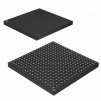
AT91SAM9G45-CU Atmel, AT91SAM9G45-CU Datasheet - Page 902

AT91SAM9G45-CU
Manufacturer Part Number
AT91SAM9G45-CU
Description
MCU ARM9 324-TFBGA
Manufacturer
Atmel
Series
AT91SAMr
Datasheets
1.AT91SAM9G45-EKES.pdf
(56 pages)
2.AT91SAM9G45-EKES.pdf
(1218 pages)
3.AT91SAM9G45-CU.pdf
(10 pages)
Specifications of AT91SAM9G45-CU
Core Processor
ARM9
Core Size
16/32-Bit
Speed
400MHz
Connectivity
EBI/EMI, Ethernet, I²C, IrDA, MMC, SPI, SSC, UART/USART, USB
Peripherals
AC'97, DMA, I²S, LCD, POR, PWM, WDT
Number Of I /o
160
Program Memory Size
64KB (64K x 8)
Program Memory Type
ROM
Ram Size
128K x 8
Voltage - Supply (vcc/vdd)
0.9 V ~ 1.1 V
Data Converters
A/D 8x10b
Oscillator Type
Internal
Operating Temperature
-40°C ~ 85°C
Package / Case
324-TFBGA
Processor Series
AT91SAMx
Core
ARM926EJ-S
Data Bus Width
32 bit
Data Ram Size
64 KB
Interface Type
I2C, SPI, UART
Maximum Clock Frequency
800 MHz
Number Of Programmable I/os
160
Number Of Timers
5
Maximum Operating Temperature
+ 85 C
Mounting Style
SMD/SMT
3rd Party Development Tools
JTRACE-ARM-2M, MDK-ARM, RL-ARM, ULINK2
Development Tools By Supplier
AT91SAM-ICE, AT91-ISP
Minimum Operating Temperature
- 40 C
On-chip Adc
10 bit
Controller Family/series
AT91
No. Of I/o's
160
Ram Memory Size
64KB
Cpu Speed
400MHz
No. Of Timers
2
Rohs Compliant
Yes
For Use With
AT91SAM9G45-EKES - KIT EVAL FOR AT91SAM9G45
Lead Free Status / RoHS Status
Lead free / RoHS Compliant
Eeprom Size
-
Lead Free Status / Rohs Status
Lead free / RoHS Compliant
Available stocks
Company
Part Number
Manufacturer
Quantity
Price
Company:
Part Number:
AT91SAM9G45-CU
Manufacturer:
ATMEL
Quantity:
1 000
Company:
Part Number:
AT91SAM9G45-CU
Manufacturer:
Atmel
Quantity:
31
Part Number:
AT91SAM9G45-CU
Manufacturer:
ATMEL/爱特梅尔
Quantity:
20 000
- Current page: 902 of 1218
- Download datasheet (19Mb)
39.4.4.3
39.4.4.4
39.4.4.5
6438F–ATARM–21-Jun-10
Memory Interface
FIFO and DMA Features
Example
Preview datapath contains a data formatter that converts 8:8:8 pixel to RGB 5:6:5 format compli-
ant with 16-bit format of the LCD controller. In general, when converting from a color channel
with more bits to one with fewer bits, formatter module discards the lower-order bits. Example:
Converting from RGB 8:8:8 to RGB 5:6:5, it discards the three LSBs from the red and blue chan-
nels, and two LSBs from the green channel. When grayscale mode is enabled, two memory
formats are supported. One mode supports 2 pixels per word, and the other mode supports 1
pixel per word.
Table 39-8.
Both preview and Codec datapaths contain FIFOs. These asynchronous buffers are used to
safely transfer formatted pixels from Pixel clock domain to AHB clock domain. A video arbiter is
used to manage FIFO thresholds and triggers a relevant DMA request through the AHB master
interface. Thus, depending on FIFO state, a specified length burst is asserted. Regarding AHB
master interface, it supports Scatter DMA mode through linked list operation. This mode of oper-
ation improves flexibility of image buffer location and allows the user to allocate two or more
frame buffers. The destination frame buffers are defined by a series of Frame Buffer Descriptors
(FBD). Each FBD controls the transfer of one entire frame and then optionally loads a further
FBD to switch the DMA operation at another frame buffer address. The FBD is defined by a
series of three words. The first one defines the current frame buffer address (named
DMA_X_ADDR register), the second defines control information (named DMA_X_CTRL regis-
ter) and the third defines the next descriptor address (named DMA_X_DSCR). DMA transfer
mode with linked list support is available for both codec and preview datapath. The data to be
transferred described by an FBD requires several burst accesses. In the example below, the use
of 2 ping-pong frame buffers is described.
The first FBD, stored at address 0x00030000, defines the location of the first frame buffer. This
address is programmed in the ISI user interface DMA_P_DSCR. To enable Descriptor fetch
operation DMA_P_CTRL register must be set to 0x00000001. LLI_0 and LLI_1 are the two
descriptors of the Linked list.
Destination Address: frame buffer ID0 0x02A000 (LLI_0.DMA_P_ADDR)
Transfer 0 Control Information, fetch and writeback: 0x00000003 (LLI_0.DMA_P_CTRL)
Next FBD address: 0x00030010 (LLI_0.DMA_P_DSCR)
Second FBD, stored at address 0x00030010, defines the location of the second frame buffer.
Destination Address: frame buffer ID1 0x0003A000 (LLI_1.DMA_P_ADDR
Transfer 1 Control information fetch and writeback: 0x00000003 (LLI_1.DMA_P_CTRL)
Next FBD address: 0x00030000, wrapping to first FBD (LLI_1.DMA_P_DSCR)
Using this technique, several frame buffers can be configured through the linked list.
illustrates a typical three frame buffer application. Frame n is mapped to frame buffer 0, frame
GS_MODE
0
1
Grayscale Memory Mapping Configuration for 12-bit Data
DATA[31:24]
P_0[11:4]
P_0[11:4]
DATA[23:16]
P_0[3:0], 0000
P_0[3:0], 0000
DATA[15:8]
P_1[11:4]
0
AT91SAM9G45
DATA[7:0]
P_1[3:0], 0000
0
Figure 39-6
902
Related parts for AT91SAM9G45-CU
Image
Part Number
Description
Manufacturer
Datasheet
Request
R

Part Number:
Description:
MCU, MPU & DSP Development Tools KICKSTART KIT FOR AT91SAM9 PLUS
Manufacturer:
IAR Systems

Part Number:
Description:
DEV KIT FOR AVR/AVR32
Manufacturer:
Atmel
Datasheet:

Part Number:
Description:
INTERVAL AND WIPE/WASH WIPER CONTROL IC WITH DELAY
Manufacturer:
ATMEL Corporation
Datasheet:

Part Number:
Description:
Low-Voltage Voice-Switched IC for Hands-Free Operation
Manufacturer:
ATMEL Corporation
Datasheet:

Part Number:
Description:
MONOLITHIC INTEGRATED FEATUREPHONE CIRCUIT
Manufacturer:
ATMEL Corporation
Datasheet:

Part Number:
Description:
AM-FM Receiver IC U4255BM-M
Manufacturer:
ATMEL Corporation
Datasheet:

Part Number:
Description:
Monolithic Integrated Feature Phone Circuit
Manufacturer:
ATMEL Corporation
Datasheet:

Part Number:
Description:
Multistandard Video-IF and Quasi Parallel Sound Processing
Manufacturer:
ATMEL Corporation
Datasheet:

Part Number:
Description:
High-performance EE PLD
Manufacturer:
ATMEL Corporation
Datasheet:

Part Number:
Description:
8-bit Flash Microcontroller
Manufacturer:
ATMEL Corporation
Datasheet:

Part Number:
Description:
2-Wire Serial EEPROM
Manufacturer:
ATMEL Corporation
Datasheet:


