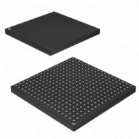
AT91SAM9G45-CU Atmel, AT91SAM9G45-CU Datasheet - Page 673

AT91SAM9G45-CU
Manufacturer Part Number
AT91SAM9G45-CU
Description
MCU ARM9 324-TFBGA
Manufacturer
Atmel
Series
AT91SAMr
Datasheets
1.AT91SAM9G45-EKES.pdf
(56 pages)
2.AT91SAM9G45-EKES.pdf
(1218 pages)
3.AT91SAM9G45-CU.pdf
(10 pages)
Specifications of AT91SAM9G45-CU
Core Processor
ARM9
Core Size
16/32-Bit
Speed
400MHz
Connectivity
EBI/EMI, Ethernet, I²C, IrDA, MMC, SPI, SSC, UART/USART, USB
Peripherals
AC'97, DMA, I²S, LCD, POR, PWM, WDT
Number Of I /o
160
Program Memory Size
64KB (64K x 8)
Program Memory Type
ROM
Ram Size
128K x 8
Voltage - Supply (vcc/vdd)
0.9 V ~ 1.1 V
Data Converters
A/D 8x10b
Oscillator Type
Internal
Operating Temperature
-40°C ~ 85°C
Package / Case
324-TFBGA
Processor Series
AT91SAMx
Core
ARM926EJ-S
Data Bus Width
32 bit
Data Ram Size
64 KB
Interface Type
I2C, SPI, UART
Maximum Clock Frequency
800 MHz
Number Of Programmable I/os
160
Number Of Timers
5
Maximum Operating Temperature
+ 85 C
Mounting Style
SMD/SMT
3rd Party Development Tools
JTRACE-ARM-2M, MDK-ARM, RL-ARM, ULINK2
Development Tools By Supplier
AT91SAM-ICE, AT91-ISP
Minimum Operating Temperature
- 40 C
On-chip Adc
10 bit
Controller Family/series
AT91
No. Of I/o's
160
Ram Memory Size
64KB
Cpu Speed
400MHz
No. Of Timers
2
Rohs Compliant
Yes
For Use With
AT91SAM9G45-EKES - KIT EVAL FOR AT91SAM9G45
Lead Free Status / RoHS Status
Lead free / RoHS Compliant
Eeprom Size
-
Lead Free Status / Rohs Status
Lead free / RoHS Compliant
Available stocks
Company
Part Number
Manufacturer
Quantity
Price
Company:
Part Number:
AT91SAM9G45-CU
Manufacturer:
ATMEL
Quantity:
1 000
Company:
Part Number:
AT91SAM9G45-CU
Manufacturer:
Atmel
Quantity:
31
Part Number:
AT91SAM9G45-CU
Manufacturer:
ATMEL/爱特梅尔
Quantity:
20 000
- Current page: 673 of 1218
- Download datasheet (19Mb)
34.7.5
34.7.5.1
34.7.5.2
34.7.6
6438F–ATARM–21-Jun-10
Frame Sync
Receive Compare Modes
Frame Sync Data
Frame Sync Edge Detection
The Transmitter and Receiver Frame Sync pins, TF and RF, can be programmed to generate
different kinds of frame synchronization signals. The Frame Sync Output Selection (FSOS) field
in the Receive Frame Mode Register (SSC_RFMR) and in the Transmit Frame Mode Register
(SSC_TFMR) are used to select the required waveform.
If a pulse waveform is selected, the Frame Sync Length (FSLEN) field in SSC_RFMR and
SSC_TFMR programs the length of the pulse, from 1 bit time up to 256 bit time.
The periodicity of the Receive and Transmit Frame Sync pulse output can be programmed
through the Period Divider Selection (PERIOD) field in SSC_RCMR and SSC_TCMR.
Frame Sync Data transmits or receives a specific tag during the Frame Sync signal.
During the Frame Sync signal, the Receiver can sample the RD line and store the data in the
Receive Sync Holding Register and the transmitter can transfer Transmit Sync Holding Register
in the Shifter Register. The data length to be sampled/shifted out during the Frame Sync signal
is programmed by the FSLEN field in SSC_RFMR/SSC_TFMR and has a maximum value of 16.
Concerning the Receive Frame Sync Data operation, if the Frame Sync Length is equal to or
lower than the delay between the start event and the actual data reception, the data sampling
operation is performed in the Receive Sync Holding Register through the Receive Shift Register.
The Transmit Frame Sync Operation is performed by the transmitter only if the bit Frame Sync
Data Enable (FSDEN) in SSC_TFMR is set. If the Frame Sync length is equal to or lower than
the delay between the start event and the actual data transmission, the normal transmission has
priority and the data contained in the Transmit Sync Holding Register is transferred in the Trans-
mit Register, then shifted out.
T h e F r a m e S y n c E d g e d e t e c t i o n i s p r o g r a m m e d b y t h e F S E D G E f i e l d i n
SSC_RFMR/SSC_TFMR. This sets the corresponding flags RXSYN/TXSYN in the SSC Status
Register (SSC_SR) on frame synchro edge detection (signals RF/TF).
Figure 34-13. Receive Compare Modes
• Programmable low or high levels during data transfer are supported.
• Programmable high levels before the start of data transfers or toggling are also supported.
(Input)
RD
RK
CMP0
(4 in This Example)
CMP1
Up to 16 Bits
FSLEN
CMP2
CMP3
Start
Ignored
STDLY
AT91SAM9G45
B0
DATLEN
B1
B2
673
Related parts for AT91SAM9G45-CU
Image
Part Number
Description
Manufacturer
Datasheet
Request
R

Part Number:
Description:
MCU, MPU & DSP Development Tools KICKSTART KIT FOR AT91SAM9 PLUS
Manufacturer:
IAR Systems

Part Number:
Description:
DEV KIT FOR AVR/AVR32
Manufacturer:
Atmel
Datasheet:

Part Number:
Description:
INTERVAL AND WIPE/WASH WIPER CONTROL IC WITH DELAY
Manufacturer:
ATMEL Corporation
Datasheet:

Part Number:
Description:
Low-Voltage Voice-Switched IC for Hands-Free Operation
Manufacturer:
ATMEL Corporation
Datasheet:

Part Number:
Description:
MONOLITHIC INTEGRATED FEATUREPHONE CIRCUIT
Manufacturer:
ATMEL Corporation
Datasheet:

Part Number:
Description:
AM-FM Receiver IC U4255BM-M
Manufacturer:
ATMEL Corporation
Datasheet:

Part Number:
Description:
Monolithic Integrated Feature Phone Circuit
Manufacturer:
ATMEL Corporation
Datasheet:

Part Number:
Description:
Multistandard Video-IF and Quasi Parallel Sound Processing
Manufacturer:
ATMEL Corporation
Datasheet:

Part Number:
Description:
High-performance EE PLD
Manufacturer:
ATMEL Corporation
Datasheet:

Part Number:
Description:
8-bit Flash Microcontroller
Manufacturer:
ATMEL Corporation
Datasheet:

Part Number:
Description:
2-Wire Serial EEPROM
Manufacturer:
ATMEL Corporation
Datasheet:


