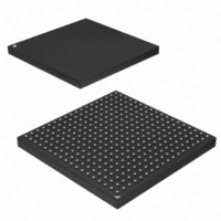
AT91SAM9G45-CU Atmel, AT91SAM9G45-CU Datasheet - Page 303

AT91SAM9G45-CU
Manufacturer Part Number
AT91SAM9G45-CU
Description
MCU ARM9 324-TFBGA
Manufacturer
Atmel
Series
AT91SAMr
Datasheets
1.AT91SAM9G45-EKES.pdf
(56 pages)
2.AT91SAM9G45-EKES.pdf
(1218 pages)
3.AT91SAM9G45-CU.pdf
(10 pages)
Specifications of AT91SAM9G45-CU
Core Processor
ARM9
Core Size
16/32-Bit
Speed
400MHz
Connectivity
EBI/EMI, Ethernet, I²C, IrDA, MMC, SPI, SSC, UART/USART, USB
Peripherals
AC'97, DMA, I²S, LCD, POR, PWM, WDT
Number Of I /o
160
Program Memory Size
64KB (64K x 8)
Program Memory Type
ROM
Ram Size
128K x 8
Voltage - Supply (vcc/vdd)
0.9 V ~ 1.1 V
Data Converters
A/D 8x10b
Oscillator Type
Internal
Operating Temperature
-40°C ~ 85°C
Package / Case
324-TFBGA
Processor Series
AT91SAMx
Core
ARM926EJ-S
Data Bus Width
32 bit
Data Ram Size
64 KB
Interface Type
I2C, SPI, UART
Maximum Clock Frequency
800 MHz
Number Of Programmable I/os
160
Number Of Timers
5
Maximum Operating Temperature
+ 85 C
Mounting Style
SMD/SMT
3rd Party Development Tools
JTRACE-ARM-2M, MDK-ARM, RL-ARM, ULINK2
Development Tools By Supplier
AT91SAM-ICE, AT91-ISP
Minimum Operating Temperature
- 40 C
On-chip Adc
10 bit
Controller Family/series
AT91
No. Of I/o's
160
Ram Memory Size
64KB
Cpu Speed
400MHz
No. Of Timers
2
Rohs Compliant
Yes
For Use With
AT91SAM9G45-EKES - KIT EVAL FOR AT91SAM9G45
Lead Free Status / RoHS Status
Lead free / RoHS Compliant
Eeprom Size
-
Lead Free Status / Rohs Status
Lead free / RoHS Compliant
Available stocks
Company
Part Number
Manufacturer
Quantity
Price
Company:
Part Number:
AT91SAM9G45-CU
Manufacturer:
ATMEL
Quantity:
1 000
Company:
Part Number:
AT91SAM9G45-CU
Manufacturer:
Atmel
Quantity:
31
Part Number:
AT91SAM9G45-CU
Manufacturer:
ATMEL/爱特梅尔
Quantity:
20 000
- Current page: 303 of 1218
- Download datasheet (19Mb)
25.5
25.6
6438F–ATARM–21-Jun-10
USB Device and Host clocks
LP-DDR/DDR2 Clock
(PMC_SCDR). The status of this clock (at least for debug purpose) can be read in the System
Clock Status Register (PMC_SCSR).
The Processor Clock PCK is enabled after a reset and is automatically re-enabled by any
enabled interrupt. The Processor Idle Mode is achieved by disabling the Processor Clock, which
is automatically re-enabled by any enabled fast or normal interrupt, or by the reset of the
product.
When the Processor Clock is disabled, the current instruction is finished before the clock is
stopped, but this does not prevent data transfers from other masters of the system bus.
The USB Device and Host High Speed ports clocks are controlled by the UDPHS and UHPHS
bits in PMC_PCER. To save power on this peripheral when they are is not used, the user can
set these bits in PMC_PCDR. The UDPHS and UHPHS bits PMC_PCSR gives the activity of
these clocks.
The PMC also provides the clocks UHP48M and UHP12M to the USB Host OHCI. The USB
Host OHCI clocks are controlled by the UHP bit in PMC_SCER. To save power on this periph-
eral when it is not used, the user can set the UHP bit in PMC_SCDR. The UHP bit in
PMC_SCSR gives the activity of this clock. The USB host OHCI requires both the 12/48 MHz
signal and the Master Clock. USBDIV field in PMC_USB register is to be programmed to 9 (divi-
sion by 10) for normal operations.
To save more power consumption user can stop UTMI PLL, in this case USB high-speed opera-
tions are not possible. Nevertheless, as the USB OHCI Input clock can be selected with USBS
bit (PLLA or UTMI PLL) in PMC_USB register, OHCI full-speed operation remain possible.
The user must program the USB OHCI Input Clock and the USBDIV divider in PMC_USB regis-
ter to generate a 48 MHz and a 12 MHz signal with an accuracy of ± 0.25%.
The Power Management Controller controls the clocks of the DDR memory. It provides SysClk
DDR internal clock. That clock is used by the DDR Controller to provide DDR control, data and
DDR clock signals.
The DDR clock can be enabled and disabled with DDRCK bit respectively in PMC_SCER and
PMC_SDER registers. At reset DDR clock is disabled to save power consumption.
The Input clock is the same as Master Clock. The Output SysClk DDR Clock is 2xMCK.
In the case MDIV = ‘00’, PCK = MCK and SysClk DDR and DDRCK clocks are not available.
If Input clock is PLLACK/PLLADIV2 the DDR Controller can drive DDR2 and LP-DDR at up to
133MHz with MDIV = ‘11’.
To save PLLA power consumption, the user can choose UPLLCK an Input clock for the system.
In this case the DDR Controller can drive LD-DDR at up to 120MHz.
AT91SAM9G45
303
Related parts for AT91SAM9G45-CU
Image
Part Number
Description
Manufacturer
Datasheet
Request
R

Part Number:
Description:
MCU, MPU & DSP Development Tools KICKSTART KIT FOR AT91SAM9 PLUS
Manufacturer:
IAR Systems

Part Number:
Description:
DEV KIT FOR AVR/AVR32
Manufacturer:
Atmel
Datasheet:

Part Number:
Description:
INTERVAL AND WIPE/WASH WIPER CONTROL IC WITH DELAY
Manufacturer:
ATMEL Corporation
Datasheet:

Part Number:
Description:
Low-Voltage Voice-Switched IC for Hands-Free Operation
Manufacturer:
ATMEL Corporation
Datasheet:

Part Number:
Description:
MONOLITHIC INTEGRATED FEATUREPHONE CIRCUIT
Manufacturer:
ATMEL Corporation
Datasheet:

Part Number:
Description:
AM-FM Receiver IC U4255BM-M
Manufacturer:
ATMEL Corporation
Datasheet:

Part Number:
Description:
Monolithic Integrated Feature Phone Circuit
Manufacturer:
ATMEL Corporation
Datasheet:

Part Number:
Description:
Multistandard Video-IF and Quasi Parallel Sound Processing
Manufacturer:
ATMEL Corporation
Datasheet:

Part Number:
Description:
High-performance EE PLD
Manufacturer:
ATMEL Corporation
Datasheet:

Part Number:
Description:
8-bit Flash Microcontroller
Manufacturer:
ATMEL Corporation
Datasheet:

Part Number:
Description:
2-Wire Serial EEPROM
Manufacturer:
ATMEL Corporation
Datasheet:


