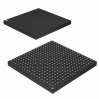
AT91SAM9G45-CU Atmel, AT91SAM9G45-CU Datasheet - Page 380

AT91SAM9G45-CU
Manufacturer Part Number
AT91SAM9G45-CU
Description
MCU ARM9 324-TFBGA
Manufacturer
Atmel
Series
AT91SAMr
Datasheets
1.AT91SAM9G45-EKES.pdf
(56 pages)
2.AT91SAM9G45-EKES.pdf
(1218 pages)
3.AT91SAM9G45-CU.pdf
(10 pages)
Specifications of AT91SAM9G45-CU
Core Processor
ARM9
Core Size
16/32-Bit
Speed
400MHz
Connectivity
EBI/EMI, Ethernet, I²C, IrDA, MMC, SPI, SSC, UART/USART, USB
Peripherals
AC'97, DMA, I²S, LCD, POR, PWM, WDT
Number Of I /o
160
Program Memory Size
64KB (64K x 8)
Program Memory Type
ROM
Ram Size
128K x 8
Voltage - Supply (vcc/vdd)
0.9 V ~ 1.1 V
Data Converters
A/D 8x10b
Oscillator Type
Internal
Operating Temperature
-40°C ~ 85°C
Package / Case
324-TFBGA
Processor Series
AT91SAMx
Core
ARM926EJ-S
Data Bus Width
32 bit
Data Ram Size
64 KB
Interface Type
I2C, SPI, UART
Maximum Clock Frequency
800 MHz
Number Of Programmable I/os
160
Number Of Timers
5
Maximum Operating Temperature
+ 85 C
Mounting Style
SMD/SMT
3rd Party Development Tools
JTRACE-ARM-2M, MDK-ARM, RL-ARM, ULINK2
Development Tools By Supplier
AT91SAM-ICE, AT91-ISP
Minimum Operating Temperature
- 40 C
On-chip Adc
10 bit
Controller Family/series
AT91
No. Of I/o's
160
Ram Memory Size
64KB
Cpu Speed
400MHz
No. Of Timers
2
Rohs Compliant
Yes
For Use With
AT91SAM9G45-EKES - KIT EVAL FOR AT91SAM9G45
Lead Free Status / RoHS Status
Lead free / RoHS Compliant
Eeprom Size
-
Lead Free Status / Rohs Status
Lead free / RoHS Compliant
Available stocks
Company
Part Number
Manufacturer
Quantity
Price
Company:
Part Number:
AT91SAM9G45-CU
Manufacturer:
ATMEL
Quantity:
1 000
Company:
Part Number:
AT91SAM9G45-CU
Manufacturer:
Atmel
Quantity:
31
Part Number:
AT91SAM9G45-CU
Manufacturer:
ATMEL/爱特梅尔
Quantity:
20 000
- Current page: 380 of 1218
- Download datasheet (19Mb)
28.3.1
28.3.2
6438F–ATARM–21-Jun-10
Write Access
Read Access
mend to utilize either 1 ECC per 256 bytes of data, 1 ECC per 512 bytes of data or 1 ECC for all
of the page.
The only configurations required for ECC are the NAND Flash or the SmartMedia page size
(528/2112/4224) and the type of correction wanted (1 ECC for all the page/1 ECC per 256 bytes
of data /1 ECC per 512 bytes of data). Page size is configured setting the PAGESIZE field in the
ECC Mode Register (ECC_MR). Type of correction is configured setting the TYPeCORRECT
field in the ECC Mode Register (ECC_MR).
ECC is automatically computed as soon as a read (00h)/write (80h) command to the NAND
Flash or the SmartMedia is detected. Read and write access must start at a page boundary.
ECC results are available as soon as the counter reaches the end of the main area. Values in
the ECC Parity Registers (ECC_PR0 to ECC_PR15) are then valid and locked until a new start
condition occurs (read/write command followed by address cycles).
Once the Flash memory page is written, the computed ECC codes are available in the ECC Par-
ity (ECC_PR0 to ECC_PR15) registers. The ECC code values must be written by the software
application in the extra area used for redundancy. The number of write accesses in the extra
area is a function of the value of the type of correction field. For example, for 1 ECC per 256
bytes of data for a page of 512 bytes, only the values of ECC_PR0 and ECC_PR1 must be writ-
ten by the software application. Other registers are meaningless.
After reading the whole data in the main area, the application must perform read accesses to the
extra area where ECC code has been previously stored. Error detection is automatically per-
formed by the ECC controller. Please note that it is mandatory to read consecutively the entire
main area and the locations where Parity and NParity values have been previously stored to let
the ECC controller perform error detection.
The application can check the ECC Status Registers (ECC_SR1/ECC_SR2) for any detected
errors. It is up to the application to correct any detected error. ECC computation can detect four
different circumstances:
• No error: XOR between the ECC computation and the ECC code stored at the end of the
• Recoverable error: Only the RECERR flags in the ECC Status registers
• ECC error: The ECCERR flag in the ECC Status Registers (ECC_SR1/ECC_SR2) are set.
• Non correctable error: The MULERR flag in the ECC Status Registers
NAND Flash or SmartMedia page is equal to 0. No error flags in the ECC Status Registers
(ECC_SR1/ECC_SR2).
(ECC_SR1/ECC_SR2) are set. The corrupted word offset in the read page is defined by the
WORDADDR field in the ECC Parity Registers (ECC_PR0 to ECC_PR15). The corrupted bit
position in the concerned word is defined in the BITADDR field in the ECC Parity Registers
(ECC_PR0 to ECC_PR15).
An error has been detected in the ECC code stored in the Flash memory. The position of the
corrupted bit can be found by the application performing an XOR between the Parity and the
NParity contained in the ECC code stored in the Flash memory.
(ECC_SR1/ECC_SR2) are set. Several unrecoverable errors have been detected in the
Flash memory page.
AT91SAM9G45
380
Related parts for AT91SAM9G45-CU
Image
Part Number
Description
Manufacturer
Datasheet
Request
R

Part Number:
Description:
MCU, MPU & DSP Development Tools KICKSTART KIT FOR AT91SAM9 PLUS
Manufacturer:
IAR Systems

Part Number:
Description:
DEV KIT FOR AVR/AVR32
Manufacturer:
Atmel
Datasheet:

Part Number:
Description:
INTERVAL AND WIPE/WASH WIPER CONTROL IC WITH DELAY
Manufacturer:
ATMEL Corporation
Datasheet:

Part Number:
Description:
Low-Voltage Voice-Switched IC for Hands-Free Operation
Manufacturer:
ATMEL Corporation
Datasheet:

Part Number:
Description:
MONOLITHIC INTEGRATED FEATUREPHONE CIRCUIT
Manufacturer:
ATMEL Corporation
Datasheet:

Part Number:
Description:
AM-FM Receiver IC U4255BM-M
Manufacturer:
ATMEL Corporation
Datasheet:

Part Number:
Description:
Monolithic Integrated Feature Phone Circuit
Manufacturer:
ATMEL Corporation
Datasheet:

Part Number:
Description:
Multistandard Video-IF and Quasi Parallel Sound Processing
Manufacturer:
ATMEL Corporation
Datasheet:

Part Number:
Description:
High-performance EE PLD
Manufacturer:
ATMEL Corporation
Datasheet:

Part Number:
Description:
8-bit Flash Microcontroller
Manufacturer:
ATMEL Corporation
Datasheet:

Part Number:
Description:
2-Wire Serial EEPROM
Manufacturer:
ATMEL Corporation
Datasheet:


