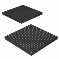
AT91SAM9G45-CU Atmel, AT91SAM9G45-CU Datasheet - Page 993

AT91SAM9G45-CU
Manufacturer Part Number
AT91SAM9G45-CU
Description
MCU ARM9 324-TFBGA
Manufacturer
Atmel
Series
AT91SAMr
Datasheets
1.AT91SAM9G45-EKES.pdf
(56 pages)
2.AT91SAM9G45-EKES.pdf
(1218 pages)
3.AT91SAM9G45-CU.pdf
(10 pages)
Specifications of AT91SAM9G45-CU
Core Processor
ARM9
Core Size
16/32-Bit
Speed
400MHz
Connectivity
EBI/EMI, Ethernet, I²C, IrDA, MMC, SPI, SSC, UART/USART, USB
Peripherals
AC'97, DMA, I²S, LCD, POR, PWM, WDT
Number Of I /o
160
Program Memory Size
64KB (64K x 8)
Program Memory Type
ROM
Ram Size
128K x 8
Voltage - Supply (vcc/vdd)
0.9 V ~ 1.1 V
Data Converters
A/D 8x10b
Oscillator Type
Internal
Operating Temperature
-40°C ~ 85°C
Package / Case
324-TFBGA
Processor Series
AT91SAMx
Core
ARM926EJ-S
Data Bus Width
32 bit
Data Ram Size
64 KB
Interface Type
I2C, SPI, UART
Maximum Clock Frequency
800 MHz
Number Of Programmable I/os
160
Number Of Timers
5
Maximum Operating Temperature
+ 85 C
Mounting Style
SMD/SMT
3rd Party Development Tools
JTRACE-ARM-2M, MDK-ARM, RL-ARM, ULINK2
Development Tools By Supplier
AT91SAM-ICE, AT91-ISP
Minimum Operating Temperature
- 40 C
On-chip Adc
10 bit
Controller Family/series
AT91
No. Of I/o's
160
Ram Memory Size
64KB
Cpu Speed
400MHz
No. Of Timers
2
Rohs Compliant
Yes
For Use With
AT91SAM9G45-EKES - KIT EVAL FOR AT91SAM9G45
Lead Free Status / RoHS Status
Lead free / RoHS Compliant
Eeprom Size
-
Lead Free Status / Rohs Status
Lead free / RoHS Compliant
Available stocks
Company
Part Number
Manufacturer
Quantity
Price
Company:
Part Number:
AT91SAM9G45-CU
Manufacturer:
ATMEL
Quantity:
1 000
Company:
Part Number:
AT91SAM9G45-CU
Manufacturer:
Atmel
Quantity:
31
Part Number:
AT91SAM9G45-CU
Manufacturer:
ATMEL/爱特梅尔
Quantity:
20 000
- Current page: 993 of 1218
- Download datasheet (19Mb)
6438F–ATARM–21-Jun-10
Note:
Note:
3. Write the starting source address in the DMAC_SADDRx register for channel x.
4. Write the channel configuration information into the DMAC_CFGx register for channel
5. Make sure that the LLI.DMAC_CTRLBx register locations of all LLIs in memory (except
6. Make sure that the LLI.DMAC_DSCRx register locations of all LLIs in memory (except
7. Make sure that the LLI.DMAC_DADDRx register location of all LLIs in memory point to
8. Make sure that the LLI.DMAC_CTLx.DONE field of the LLI.DMAC_CTRLA register
9. If source picture-in-picture is enabled (DMAC_CTRLBx.SPIP is enabled), program the
10. If destination picture-in-picture is enabled (DMAC_CTRLBx.DPIP is enabled), program
11. Clear any pending interrupts on the channel from the previous DMAC transfer by read-
12. Program the DMAC_CTLx, DMAC_CFGx registers according to Row 6 as shown in
13. Program the DMAC_DSCRx register with DMAC_DSCRx(0), the pointer to the first
14. Finally, enable the channel by writing a ‘1’ to the DMAC_CHER.ENABLE[n] bit where n
15. The DMAC fetches the first LLI from the location pointed to by DMAC_DSCRx(0).
16. Source and destination request single and chunk DMAC transactions to transfer the
17. The DMAC_CTRLAx register is written out to system memory. The DMAC_CTRLAx
x.
a. Designate the handshaking interface type (hardware or software) for the source
b. If the hardware handshaking interface is activated for the source or destination
the last) are set as shown in Row 6 of
LLI.DMAC_CTRLBx register of the last Linked List item must be set as described in
Row 1 of
list items.
the last) are non-zero and point to the next Linked List Item.
the start destination buffer address proceeding that LLI fetch.
locations of all LLIs in memory is cleared.
DMAC_SPIPx register for channel x.
the DMAC_DPIPx register for channel x.
ing to the DMAC_EBCISR register.
Table 41-2 on page
Linked List item.
is the channel number. The transfer is performed. Make sure that bit 0 of the DMAC_EN
register is enabled.
buffer of data (assuming non-memory peripherals). DMAC acknowledges at the com-
pletion of every transaction (chunk and single) in the buffer and carry out the buffer
transfer.
register is written out to the same location on the same layer
(DMAC_DSCRx.DSCR_IF) where it was originally fetched, that is the location of the
DMAC_CTRLAx register of the linked list item fetched prior to the start of the buffer
The values in the LLI.DMAC_SADDRx register locations of each of the Linked List Items (LLIs)
setup up in memory, although fetched during a LLI fetch, are not used.
The LLI.DMAC_SADDRx, LLI.DMAC_DADDRx, LLI. DMAC_LLPx LLI.DMAC_CTRLAx and
LLI.DMAC_CTRLBx registers are fetched. The LLI.DMAC_SADDRx register although fetched is
not used.
and destination peripherals. This is not required for memory. This step requires pro-
gramming the SRC_H2SEL/DST_H2SEL bits, respectively. Writing a ‘1’ activates
the hardware handshaking interface to handle source/destination requests for the
specific channel. Writing a ‘0’ activates the software handshaking interface
source/destination requests.
peripheral, assign handshaking interface to the source and destination peripheral.
This requires programming the SRC_PER and DST_PER bits, respectively.
Table
41-2.
982.
Figure 41-5 on page 981
Table 41-2 on page 982
shows a Linked List example with two
AT91SAM9G45
while the
993
Related parts for AT91SAM9G45-CU
Image
Part Number
Description
Manufacturer
Datasheet
Request
R

Part Number:
Description:
MCU, MPU & DSP Development Tools KICKSTART KIT FOR AT91SAM9 PLUS
Manufacturer:
IAR Systems

Part Number:
Description:
DEV KIT FOR AVR/AVR32
Manufacturer:
Atmel
Datasheet:

Part Number:
Description:
INTERVAL AND WIPE/WASH WIPER CONTROL IC WITH DELAY
Manufacturer:
ATMEL Corporation
Datasheet:

Part Number:
Description:
Low-Voltage Voice-Switched IC for Hands-Free Operation
Manufacturer:
ATMEL Corporation
Datasheet:

Part Number:
Description:
MONOLITHIC INTEGRATED FEATUREPHONE CIRCUIT
Manufacturer:
ATMEL Corporation
Datasheet:

Part Number:
Description:
AM-FM Receiver IC U4255BM-M
Manufacturer:
ATMEL Corporation
Datasheet:

Part Number:
Description:
Monolithic Integrated Feature Phone Circuit
Manufacturer:
ATMEL Corporation
Datasheet:

Part Number:
Description:
Multistandard Video-IF and Quasi Parallel Sound Processing
Manufacturer:
ATMEL Corporation
Datasheet:

Part Number:
Description:
High-performance EE PLD
Manufacturer:
ATMEL Corporation
Datasheet:

Part Number:
Description:
8-bit Flash Microcontroller
Manufacturer:
ATMEL Corporation
Datasheet:

Part Number:
Description:
2-Wire Serial EEPROM
Manufacturer:
ATMEL Corporation
Datasheet:


