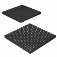
AT91SAM9G45-CU Atmel, AT91SAM9G45-CU Datasheet - Page 46

AT91SAM9G45-CU
Manufacturer Part Number
AT91SAM9G45-CU
Description
MCU ARM9 324-TFBGA
Manufacturer
Atmel
Series
AT91SAMr
Datasheets
1.AT91SAM9G45-EKES.pdf
(56 pages)
2.AT91SAM9G45-EKES.pdf
(1218 pages)
3.AT91SAM9G45-CU.pdf
(10 pages)
Specifications of AT91SAM9G45-CU
Core Processor
ARM9
Core Size
16/32-Bit
Speed
400MHz
Connectivity
EBI/EMI, Ethernet, I²C, IrDA, MMC, SPI, SSC, UART/USART, USB
Peripherals
AC'97, DMA, I²S, LCD, POR, PWM, WDT
Number Of I /o
160
Program Memory Size
64KB (64K x 8)
Program Memory Type
ROM
Ram Size
128K x 8
Voltage - Supply (vcc/vdd)
0.9 V ~ 1.1 V
Data Converters
A/D 8x10b
Oscillator Type
Internal
Operating Temperature
-40°C ~ 85°C
Package / Case
324-TFBGA
Processor Series
AT91SAMx
Core
ARM926EJ-S
Data Bus Width
32 bit
Data Ram Size
64 KB
Interface Type
I2C, SPI, UART
Maximum Clock Frequency
800 MHz
Number Of Programmable I/os
160
Number Of Timers
5
Maximum Operating Temperature
+ 85 C
Mounting Style
SMD/SMT
3rd Party Development Tools
JTRACE-ARM-2M, MDK-ARM, RL-ARM, ULINK2
Development Tools By Supplier
AT91SAM-ICE, AT91-ISP
Minimum Operating Temperature
- 40 C
On-chip Adc
10 bit
Controller Family/series
AT91
No. Of I/o's
160
Ram Memory Size
64KB
Cpu Speed
400MHz
No. Of Timers
2
Rohs Compliant
Yes
For Use With
AT91SAM9G45-EKES - KIT EVAL FOR AT91SAM9G45
Lead Free Status / RoHS Status
Lead free / RoHS Compliant
Eeprom Size
-
Lead Free Status / Rohs Status
Lead free / RoHS Compliant
Available stocks
Company
Part Number
Manufacturer
Quantity
Price
Company:
Part Number:
AT91SAM9G45-CU
Manufacturer:
ATMEL
Quantity:
1 000
Company:
Part Number:
AT91SAM9G45-CU
Manufacturer:
Atmel
Quantity:
31
Part Number:
AT91SAM9G45-CU
Manufacturer:
ATMEL/爱特梅尔
Quantity:
20 000
- Current page: 46 of 1218
- Download datasheet (19Mb)
9.7
9.7.1
9.7.2
9.7.2.1
46
Caches and Write Buffer
AT91SAM9G45
Instruction Cache (ICache)
Data Cache (DCache) and Write Buffer
DCache
The ARM926EJ-S contains a 32K Byte Instruction Cache (ICache), a 32K Byte Data Cache
(DCache), and a write buffer. Although the ICache and DCache share common features, each
still has some specific mechanisms.
The caches (ICache and DCache) are four-way set associative, addressed, indexed and tagged
using the Modified Virtual Address (MVA), with a cache line length of eight words with two dirty
bits for the DCache. The ICache and DCache provide mechanisms for cache lockdown, cache
pollution control, and line replacement.
A new feature is now supported by ARM926EJ-S caches called allocate on read-miss commonly
known as wrapping. This feature enables the caches to perform critical word first cache refilling.
This means that when a request for a word causes a read-miss, the cache performs an AHB
access. Instead of loading the whole line (eight words), the cache loads the critical word first, so
the processor can reach it quickly, and then the remaining words, no matter where the word is
located in the line.
The caches and the write buffer are controlled by the CP15 register 1 (Control), CP15 register 7
(cache operations) and CP15 register 9 (cache lockdown).
The ICache caches fetched instructions to be executed by the processor. The ICache can be
enabled by writing 1 to I bit of the CP15 Register 1 and disabled by writing 0 to this same bit.
When the MMU is enabled, all instruction fetches are subject to translation and permission
checks. If the MMU is disabled, all instructions fetches are cachable, no protection checks are
made and the physical address is flat-mapped to the modified virtual address. With the MVA use
disabled, context switching incurs ICache cleaning and/or invalidating.
When the ICache is disabled, all instruction fetches appear on external memory (AHB) (see
Tables 4-1 and 4-2 in page 4-4 in ARM926EJ-S TRM).
On reset, the ICache entries are invalidated and the ICache is disabled. For best performance,
ICache should be enabled as soon as possible after reset.
ARM926EJ-S includes a DCache and a write buffer to reduce the effect of main memory band-
width and latency on data access performance. The operations of DCache and write buffer are
closely connected.
The DCache needs the MMU to be enabled. All data accesses are subject to MMU permission
and translation checks. Data accesses that are aborted by the MMU do not cause linefills or data
accesses to appear on the AMBA ASB interface. If the MMU is disabled, all data accesses are
noncachable, nonbufferable, with no protection checks, and appear on the AHB bus. All
addresses are flat-mapped, VA = MVA = PA, which incurs DCache cleaning and/or invalidating
every time a context switch occurs.
The DCache stores the Physical Address Tag (PA Tag) from which every line was loaded and
uses it when writing modified lines back to external memory. This means that the MMU is not
involved in write-back operations.
Each line (8 words) in the DCache has two dirty bits, one for the first four words and the other
one for the second four words. These bits, if set, mark the associated half-lines as dirty. If the
6438F–ATARM–21-Jun-10
Related parts for AT91SAM9G45-CU
Image
Part Number
Description
Manufacturer
Datasheet
Request
R

Part Number:
Description:
MCU, MPU & DSP Development Tools KICKSTART KIT FOR AT91SAM9 PLUS
Manufacturer:
IAR Systems

Part Number:
Description:
DEV KIT FOR AVR/AVR32
Manufacturer:
Atmel
Datasheet:

Part Number:
Description:
INTERVAL AND WIPE/WASH WIPER CONTROL IC WITH DELAY
Manufacturer:
ATMEL Corporation
Datasheet:

Part Number:
Description:
Low-Voltage Voice-Switched IC for Hands-Free Operation
Manufacturer:
ATMEL Corporation
Datasheet:

Part Number:
Description:
MONOLITHIC INTEGRATED FEATUREPHONE CIRCUIT
Manufacturer:
ATMEL Corporation
Datasheet:

Part Number:
Description:
AM-FM Receiver IC U4255BM-M
Manufacturer:
ATMEL Corporation
Datasheet:

Part Number:
Description:
Monolithic Integrated Feature Phone Circuit
Manufacturer:
ATMEL Corporation
Datasheet:

Part Number:
Description:
Multistandard Video-IF and Quasi Parallel Sound Processing
Manufacturer:
ATMEL Corporation
Datasheet:

Part Number:
Description:
High-performance EE PLD
Manufacturer:
ATMEL Corporation
Datasheet:

Part Number:
Description:
8-bit Flash Microcontroller
Manufacturer:
ATMEL Corporation
Datasheet:

Part Number:
Description:
2-Wire Serial EEPROM
Manufacturer:
ATMEL Corporation
Datasheet:


