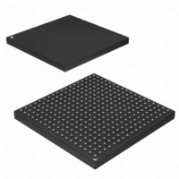
AT91SAM9G45-CU Atmel, AT91SAM9G45-CU Datasheet - Page 1121

AT91SAM9G45-CU
Manufacturer Part Number
AT91SAM9G45-CU
Description
MCU ARM9 324-TFBGA
Manufacturer
Atmel
Series
AT91SAMr
Datasheets
1.AT91SAM9G45-EKES.pdf
(56 pages)
2.AT91SAM9G45-EKES.pdf
(1218 pages)
3.AT91SAM9G45-CU.pdf
(10 pages)
Specifications of AT91SAM9G45-CU
Core Processor
ARM9
Core Size
16/32-Bit
Speed
400MHz
Connectivity
EBI/EMI, Ethernet, I²C, IrDA, MMC, SPI, SSC, UART/USART, USB
Peripherals
AC'97, DMA, I²S, LCD, POR, PWM, WDT
Number Of I /o
160
Program Memory Size
64KB (64K x 8)
Program Memory Type
ROM
Ram Size
128K x 8
Voltage - Supply (vcc/vdd)
0.9 V ~ 1.1 V
Data Converters
A/D 8x10b
Oscillator Type
Internal
Operating Temperature
-40°C ~ 85°C
Package / Case
324-TFBGA
Processor Series
AT91SAMx
Core
ARM926EJ-S
Data Bus Width
32 bit
Data Ram Size
64 KB
Interface Type
I2C, SPI, UART
Maximum Clock Frequency
800 MHz
Number Of Programmable I/os
160
Number Of Timers
5
Maximum Operating Temperature
+ 85 C
Mounting Style
SMD/SMT
3rd Party Development Tools
JTRACE-ARM-2M, MDK-ARM, RL-ARM, ULINK2
Development Tools By Supplier
AT91SAM-ICE, AT91-ISP
Minimum Operating Temperature
- 40 C
On-chip Adc
10 bit
Controller Family/series
AT91
No. Of I/o's
160
Ram Memory Size
64KB
Cpu Speed
400MHz
No. Of Timers
2
Rohs Compliant
Yes
For Use With
AT91SAM9G45-EKES - KIT EVAL FOR AT91SAM9G45
Lead Free Status / RoHS Status
Lead free / RoHS Compliant
Eeprom Size
-
Lead Free Status / Rohs Status
Lead free / RoHS Compliant
Available stocks
Company
Part Number
Manufacturer
Quantity
Price
Company:
Part Number:
AT91SAM9G45-CU
Manufacturer:
ATMEL
Quantity:
1 000
Company:
Part Number:
AT91SAM9G45-CU
Manufacturer:
Atmel
Quantity:
31
Part Number:
AT91SAM9G45-CU
Manufacturer:
ATMEL/爱特梅尔
Quantity:
20 000
- Current page: 1121 of 1218
- Download datasheet (19Mb)
6438F–ATARM–21-Jun-10
• Configure the DMA Controller. The user should configure the base address of the display
• Finally, enable the LCD Controller Core by writing a “1” in the LCD_PWR field of the
buffer memory, the size of the AHB transaction and the size of the display image in memory.
When the DMA is configured the user should enable the DMA. To do so the user should
configure the following registers:
PWRCON register and do any other action that may be required to turn the LCD module on.
– LCDCON2 register: Program its fields following their descriptions in the LCD
– LCDTIM1 and LCDTIM2 registers: Program their fields according to the datasheet of
– LCDFRMCFG register: program the dimensions of the LCD module used.
– LCDFIFO register: To program it, use the formula in section
– LCDMVAL register: Its configuration depends on the LCD Module used and should
– DP1_2 to DP6_7 registers: they are only used for STN displays. They contain the
– PWRCON Register: this register controls the power-up sequence of the LCD, so
– CONTRAST_CTR and CONTRAST_VAL: use this registers to adjust the contrast of
– DMABADDR1 and DMABADDR2 registers: In single scan mode only DMABADDR1
– DMAFRMCFG register: Program the FRMSIZE field. Note that in dual scan mode
– DMACON register: Once both the LCD Controller Core and the DMA Controller have
– DMA2DCFG register: Required only in 2D memory addressing mode (see
Controller User Interface section below and considering the type of LCD module
used and the desired working mode. Consider that not all combinations are possible.
the LCD module used and with the help of the Timegen section in page 10. Note that
some fields are not applicable to STN modules and must be programmed with 0
values. Note also that there is a limitation on the minimum value of VHDLY, HPW,
HBP that depends on the configuration of the LCDC.
be tuned to improve the image quality in the display
dithering patterns used to generate gray shades or colors in these modules. They
are loaded with recommended patterns at reset, so it is not necessary to write
anything on them. They can be used to improve the image quality in the display by
tuning the patterns in each application.
take care to use it properly. Do not enable the LCD (writing a 1 in LCD_PWR field)
until the previous steps and the configuration of the DMA have been finished.
the display, when the LCDCC line is used.
register must be configured with the base address of the display buffer in memory. In
dual scan mode DMABADDR1 should be configured with the base address of the
Upper Panel display buffer and DMABADDR2 should be configured with the base
address of the Lower Panel display buffer.
the vertical size to use in the calculation is that of each panel. Respect to the
BRSTLN field, a recommended value is a 4-word burst.
been configured, enable the DMA Controller by writing a “1” to the DMAEN field of
this register. If using a dual scan module or the 2D addressing feature, do not forget
to write the DMAUPDT bit after every change to the set of DMA configuration values.
Memory Addressing” on page
1122).
(See “Timegen” on page
AT91SAM9G45
“FIFO” on page 1102
“2D
1108.)
1121
Related parts for AT91SAM9G45-CU
Image
Part Number
Description
Manufacturer
Datasheet
Request
R

Part Number:
Description:
MCU, MPU & DSP Development Tools KICKSTART KIT FOR AT91SAM9 PLUS
Manufacturer:
IAR Systems

Part Number:
Description:
DEV KIT FOR AVR/AVR32
Manufacturer:
Atmel
Datasheet:

Part Number:
Description:
INTERVAL AND WIPE/WASH WIPER CONTROL IC WITH DELAY
Manufacturer:
ATMEL Corporation
Datasheet:

Part Number:
Description:
Low-Voltage Voice-Switched IC for Hands-Free Operation
Manufacturer:
ATMEL Corporation
Datasheet:

Part Number:
Description:
MONOLITHIC INTEGRATED FEATUREPHONE CIRCUIT
Manufacturer:
ATMEL Corporation
Datasheet:

Part Number:
Description:
AM-FM Receiver IC U4255BM-M
Manufacturer:
ATMEL Corporation
Datasheet:

Part Number:
Description:
Monolithic Integrated Feature Phone Circuit
Manufacturer:
ATMEL Corporation
Datasheet:

Part Number:
Description:
Multistandard Video-IF and Quasi Parallel Sound Processing
Manufacturer:
ATMEL Corporation
Datasheet:

Part Number:
Description:
High-performance EE PLD
Manufacturer:
ATMEL Corporation
Datasheet:

Part Number:
Description:
8-bit Flash Microcontroller
Manufacturer:
ATMEL Corporation
Datasheet:

Part Number:
Description:
2-Wire Serial EEPROM
Manufacturer:
ATMEL Corporation
Datasheet:


