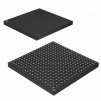
AT91SAM9G45-CU Atmel, AT91SAM9G45-CU Datasheet - Page 438

AT91SAM9G45-CU
Manufacturer Part Number
AT91SAM9G45-CU
Description
MCU ARM9 324-TFBGA
Manufacturer
Atmel
Series
AT91SAMr
Datasheets
1.AT91SAM9G45-EKES.pdf
(56 pages)
2.AT91SAM9G45-EKES.pdf
(1218 pages)
3.AT91SAM9G45-CU.pdf
(10 pages)
Specifications of AT91SAM9G45-CU
Core Processor
ARM9
Core Size
16/32-Bit
Speed
400MHz
Connectivity
EBI/EMI, Ethernet, I²C, IrDA, MMC, SPI, SSC, UART/USART, USB
Peripherals
AC'97, DMA, I²S, LCD, POR, PWM, WDT
Number Of I /o
160
Program Memory Size
64KB (64K x 8)
Program Memory Type
ROM
Ram Size
128K x 8
Voltage - Supply (vcc/vdd)
0.9 V ~ 1.1 V
Data Converters
A/D 8x10b
Oscillator Type
Internal
Operating Temperature
-40°C ~ 85°C
Package / Case
324-TFBGA
Processor Series
AT91SAMx
Core
ARM926EJ-S
Data Bus Width
32 bit
Data Ram Size
64 KB
Interface Type
I2C, SPI, UART
Maximum Clock Frequency
800 MHz
Number Of Programmable I/os
160
Number Of Timers
5
Maximum Operating Temperature
+ 85 C
Mounting Style
SMD/SMT
3rd Party Development Tools
JTRACE-ARM-2M, MDK-ARM, RL-ARM, ULINK2
Development Tools By Supplier
AT91SAM-ICE, AT91-ISP
Minimum Operating Temperature
- 40 C
On-chip Adc
10 bit
Controller Family/series
AT91
No. Of I/o's
160
Ram Memory Size
64KB
Cpu Speed
400MHz
No. Of Timers
2
Rohs Compliant
Yes
For Use With
AT91SAM9G45-EKES - KIT EVAL FOR AT91SAM9G45
Lead Free Status / RoHS Status
Lead free / RoHS Compliant
Eeprom Size
-
Lead Free Status / Rohs Status
Lead free / RoHS Compliant
Available stocks
Company
Part Number
Manufacturer
Quantity
Price
Company:
Part Number:
AT91SAM9G45-CU
Manufacturer:
ATMEL
Quantity:
1 000
Company:
Part Number:
AT91SAM9G45-CU
Manufacturer:
Atmel
Quantity:
31
Part Number:
AT91SAM9G45-CU
Manufacturer:
ATMEL/爱特梅尔
Quantity:
20 000
- Current page: 438 of 1218
- Download datasheet (19Mb)
Figure 29-13. Slave Mode Functional Bloc Diagram
438
AT91SAM9G45
SPCK
MOSI
NSS
The bits are shifted out on the MISO line and sampled on the MOSI line.
(For more information on BITS field, see also, the
“SPI Chip Select Register” on page
When all the bits are processed, the received data is transferred in the Receive Data Register
and the RDRF bit rises. If the SPI_RDR (Receive Data Register) has not been read before new
data is received, the Overrun Error bit (OVRES) in SPI_SR is set. As long as this flag is set, data
is loaded in SPI_RDR. The user has to read the status register to clear the OVRES bit.
When a transfer starts, the data shifted out is the data present in the Shift Register. If no data
has been written in the Transmit Data Register (SPI_TDR), the last data received is transferred.
If no data has been received since the last reset, all bits are transmitted low, as the Shift Regis-
ter resets at 0.
When a first data is written in SPI_TDR, it is transferred immediately in the Shift Register and the
TDRE bit rises. If new data is written, it remains in SPI_TDR until a transfer occurs, i.e. NSS falls
and there is a valid clock on the SPCK pin. When the transfer occurs, the last data written in
SPI_TDR is transferred in the Shift Register and the TDRE bit rises. This enables frequent
updates of critical variables with single transfers.
Then, a new data is loaded in the Shift Register from the Transmit Data Register. In case no
character is ready to be transmitted, i.e. no character has been written in SPI_TDR since the last
load from SPI_TDR to the Shift Register, the Shift Register is not modified and the last received
character is retransmitted.
Figure 29-13
SPIDIS
SPIEN
SPIENS
SPI_CSR0
shows a block diagram of the SPI when operating in Slave Mode.
LSB
NCPHA
CPOL
BITS
Shift Register
Clock
SPI
SPI_RDR
SPI_TDR
450.)
RD
TD
(Note:)
MSB
below the register table;
OVRES
RDRF
TDRE
MISO
6438F–ATARM–21-Jun-10
Section 29.8.9
Related parts for AT91SAM9G45-CU
Image
Part Number
Description
Manufacturer
Datasheet
Request
R

Part Number:
Description:
MCU, MPU & DSP Development Tools KICKSTART KIT FOR AT91SAM9 PLUS
Manufacturer:
IAR Systems

Part Number:
Description:
DEV KIT FOR AVR/AVR32
Manufacturer:
Atmel
Datasheet:

Part Number:
Description:
INTERVAL AND WIPE/WASH WIPER CONTROL IC WITH DELAY
Manufacturer:
ATMEL Corporation
Datasheet:

Part Number:
Description:
Low-Voltage Voice-Switched IC for Hands-Free Operation
Manufacturer:
ATMEL Corporation
Datasheet:

Part Number:
Description:
MONOLITHIC INTEGRATED FEATUREPHONE CIRCUIT
Manufacturer:
ATMEL Corporation
Datasheet:

Part Number:
Description:
AM-FM Receiver IC U4255BM-M
Manufacturer:
ATMEL Corporation
Datasheet:

Part Number:
Description:
Monolithic Integrated Feature Phone Circuit
Manufacturer:
ATMEL Corporation
Datasheet:

Part Number:
Description:
Multistandard Video-IF and Quasi Parallel Sound Processing
Manufacturer:
ATMEL Corporation
Datasheet:

Part Number:
Description:
High-performance EE PLD
Manufacturer:
ATMEL Corporation
Datasheet:

Part Number:
Description:
8-bit Flash Microcontroller
Manufacturer:
ATMEL Corporation
Datasheet:

Part Number:
Description:
2-Wire Serial EEPROM
Manufacturer:
ATMEL Corporation
Datasheet:


