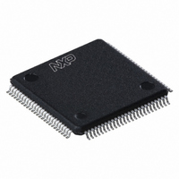
LPC1767FBD100,551 NXP Semiconductors, LPC1767FBD100,551 Datasheet - Page 111

LPC1767FBD100,551
Manufacturer Part Number
LPC1767FBD100,551
Description
IC ARM CORTEX MCU 512K 100-LQFP
Manufacturer
NXP Semiconductors
Series
LPC17xxr
Datasheets
1.LPC1767FBD100551.pdf
(2 pages)
2.LPC1767FBD100551.pdf
(840 pages)
3.LPC1767FBD100551.pdf
(65 pages)
Specifications of LPC1767FBD100,551
Core Processor
ARM® Cortex-M3™
Core Size
32-Bit
Speed
100MHz
Connectivity
Ethernet, I²C, IrDA, Microwire, SPI, SSI, UART/USART
Peripherals
Brown-out Detect/Reset, DMA, I²S, Motor Control PWM, POR, PWM, WDT
Number Of I /o
70
Program Memory Size
512KB (512K x 8)
Program Memory Type
FLASH
Ram Size
64K x 8
Voltage - Supply (vcc/vdd)
2.4 V ~ 3.6 V
Data Converters
A/D 8x12b, D/A 1x10b
Oscillator Type
Internal
Operating Temperature
-40°C ~ 85°C
Package / Case
100-LQFP
Processor Series
LPC17
Core
ARM Cortex M3
3rd Party Development Tools
MDK-ARM, RL-ARM, ULINK2, MCB1760, MCB1760U, MCB1760UME
For Use With
622-1005 - USB IN-CIRCUIT PROG ARM7 LPC2K
Lead Free Status / RoHS Status
Lead free / RoHS Compliant
Eeprom Size
-
Lead Free Status / Rohs Status
Details
Other names
568-4967
935289808551
935289808551
Available stocks
Company
Part Number
Manufacturer
Quantity
Price
Company:
Part Number:
LPC1767FBD100,551
Manufacturer:
NXP Semiconductors
Quantity:
10 000
- Current page: 111 of 840
- Download datasheet (6Mb)
NXP Semiconductors
UM10360
User manual
8.5.6 Pin Function Select Register 7 (PINSEL7 - 0x4002 C01C)
8.5.7 Pin Function Select Register 9 (PINSEL9 - 0x4002 C024)
8.5.8 Pin Function Select Register 10 (PINSEL10 - 0x4002 C028)
The PINSEL7 register controls the functions of the upper half of Port 3. The direction
control bit in the FIO3DIR register is effective only when the GPIO function is selected for
a pin. For other functions, direction is controlled automatically.
Table 84.
[1]
The PINSEL9 register controls the functions of the upper half of Port 4. The direction
control bit in the FIO4DIR register is effective only when the GPIO function is selected for
a pin. For other functions, direction is controlled automatically.
Table 85.
Only bit 3 of this register is used to control the Trace function on pins P2.2 through P2.6.
Table 86.
PINSEL7 Pin
17:0
19:18
21:20
31:22
PINSEL9 Pin
23:0
25:24
27:26
31:28
Bit
2:0
3
31:4
Not available on 80-pin package.
Symbol
-
GPIO/TRACE
-
name
-
P3.25
P3.26
-
name
-
P4.28
P4.29
-
Pin function select register 7 (PINSEL7 - address 0x4002 C01C) bit description
Pin function select register 9 (PINSEL9 - address 0x4002 C024) bit description
Pin function select register 10 (PINSEL10 - address 0x4002 C028) bit description
All information provided in this document is subject to legal disclaimers.
[1]
[1]
Function when
00
Reserved
GPIO Port 4.28
GPIO Port 4.29
Reserved
Function when
00
Reserved
GPIO Port 3.25
GPIO Port 3.26
Reserved
Value Description
-
0
1
-
Rev. 2 — 19 August 2010
Reserved. Software should not write 1 to these bits. NA
TPIU interface pins control.
TPIU interface is disabled.
TPIU interface is enabled. TPIU signals are
available on the pins hosting them regardless of the
PINSEL4 content.
Reserved. Software should not write 1 to these bits. NA
Function
when 01
Reserved
RX_MCLK
TX_MCLK
Reserved
Reserved
Function
when 01
Reserved
STCLK
Reserved
Chapter 8: LPC17xx Pin connect block
Function
when 10
Reserved
MAT2.0
MAT2.1
Reserved
Function
when 10
Reserved
MAT0.0
MAT0.1
Reserved
Function
when 11
Reserved
TXD3
RXD3
Reserved
Function
when 11
Reserved
PWM1.2
PWM1.3
Reserved
UM10360
© NXP B.V. 2010. All rights reserved.
Reset
value
0
Reset
value
00
00
00
00
Reset
value
0
00
00
0
111 of 840
Related parts for LPC1767FBD100,551
Image
Part Number
Description
Manufacturer
Datasheet
Request
R

Part Number:
Description:
32-bit ARM Cortex-M3 microcontroller; up to 512 kB flash and 64 kB SRAM with Ethernet, USB 2.0 Host/Device/OTG, CAN
Manufacturer:
NXP [NXP Semiconductors]
Datasheet:
Part Number:
Description:
NXP Semiconductors designed the LPC2420/2460 microcontroller around a 16-bit/32-bitARM7TDMI-S CPU core with real-time debug interfaces that include both JTAG andembedded trace
Manufacturer:
NXP Semiconductors
Datasheet:

Part Number:
Description:
NXP Semiconductors designed the LPC2458 microcontroller around a 16-bit/32-bitARM7TDMI-S CPU core with real-time debug interfaces that include both JTAG andembedded trace
Manufacturer:
NXP Semiconductors
Datasheet:
Part Number:
Description:
NXP Semiconductors designed the LPC2468 microcontroller around a 16-bit/32-bitARM7TDMI-S CPU core with real-time debug interfaces that include both JTAG andembedded trace
Manufacturer:
NXP Semiconductors
Datasheet:
Part Number:
Description:
NXP Semiconductors designed the LPC2470 microcontroller, powered by theARM7TDMI-S core, to be a highly integrated microcontroller for a wide range ofapplications that require advanced communications and high quality graphic displays
Manufacturer:
NXP Semiconductors
Datasheet:
Part Number:
Description:
NXP Semiconductors designed the LPC2478 microcontroller, powered by theARM7TDMI-S core, to be a highly integrated microcontroller for a wide range ofapplications that require advanced communications and high quality graphic displays
Manufacturer:
NXP Semiconductors
Datasheet:
Part Number:
Description:
The Philips Semiconductors XA (eXtended Architecture) family of 16-bit single-chip microcontrollers is powerful enough to easily handle the requirements of high performance embedded applications, yet inexpensive enough to compete in the market for hi
Manufacturer:
NXP Semiconductors
Datasheet:
Part Number:
Description:
The XA-S3 device is a member of Philips Semiconductors? XA(eXtended Architecture) family of high performance 16-bitsingle-chip microcontrollers
Manufacturer:
NXP Semiconductors
Datasheet:

Part Number:
Description:
The NXP BlueStreak LH75401/LH75411 family consists of two low-cost 16/32-bit System-on-Chip (SoC) devices
Manufacturer:
NXP Semiconductors
Datasheet:

Part Number:
Description:
The NXP LPC3130/3131 combine an 180 MHz ARM926EJ-S CPU core, high-speed USB2
Manufacturer:
NXP Semiconductors
Datasheet:

Part Number:
Description:
The NXP LPC3141 combine a 270 MHz ARM926EJ-S CPU core, High-speed USB 2
Manufacturer:
NXP Semiconductors

Part Number:
Description:
The NXP LPC3143 combine a 270 MHz ARM926EJ-S CPU core, High-speed USB 2
Manufacturer:
NXP Semiconductors

Part Number:
Description:
The NXP LPC3152 combines an 180 MHz ARM926EJ-S CPU core, High-speed USB 2
Manufacturer:
NXP Semiconductors

Part Number:
Description:
The NXP LPC3154 combines an 180 MHz ARM926EJ-S CPU core, High-speed USB 2
Manufacturer:
NXP Semiconductors


