DF2437FV Renesas Electronics America, DF2437FV Datasheet - Page 13
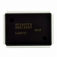
DF2437FV
Manufacturer Part Number
DF2437FV
Description
IC H8S/2437 MCU FLASH 128QFP
Manufacturer
Renesas Electronics America
Series
H8® H8S/2400r
Specifications of DF2437FV
Core Processor
H8S/2600
Core Size
16-Bit
Speed
20MHz
Connectivity
I²C, SCI
Peripherals
POR, PWM, WDT
Number Of I /o
85
Program Memory Size
256KB (256K x 8)
Program Memory Type
FLASH
Ram Size
16K x 8
Voltage - Supply (vcc/vdd)
3 V ~ 3.6 V
Data Converters
A/D 16x10b
Oscillator Type
Internal
Operating Temperature
-20°C ~ 75°C
Package / Case
128-QFP
Lead Free Status / RoHS Status
Lead free / RoHS Compliant
Eeprom Size
-
Available stocks
Company
Part Number
Manufacturer
Quantity
Price
Company:

Part Number:
DF2437FV
Manufacturer:
Renesas Electronics America
Quantity:
10 000


5.5
5.6
5.7
Section 6 Bus Controller (BSC)........................................................................ 93
6.1
6.2
6.3
6.4
6.5
6.6
Section 7 I/O Ports ............................................................................................ 133
7.1
7.2
Interrupt Exception Handling Vector Table......................................................................77
Interrupt Control Modes and Interrupt Operation .............................................................82
5.6.1
5.6.2
5.6.3
5.6.4
Usage Notes ......................................................................................................................90
5.7.1
5.7.2
5.7.3
5.7.4
5.7.5
5.7.6
Features .............................................................................................................................93
Input/Output Pins .............................................................................................................. 95
Register Descriptions ........................................................................................................96
6.3.1
6.3.2
Bus Control .......................................................................................................................99
6.4.1
6.4.2
6.4.3
6.4.4
6.4.5
Bus Interface .....................................................................................................................104
6.5.1
6.5.2
6.5.3
6.5.4
6.5.5
Idle Cycle ..........................................................................................................................130
Port 0.................................................................................................................................139
7.1.1
7.1.2
Port 1.................................................................................................................................141
7.2.1
7.2.2
7.2.3
Interrupt Control Mode 0 .....................................................................................82
Interrupt Control Mode 2 .....................................................................................84
Interrupt Exception Handling Sequence ..............................................................86
Interrupt Response Times ....................................................................................88
Contention between Interrupt Generation and Disabling.....................................90
Instructions that Disable Interrupts ......................................................................91
Times when Interrupts are Disabled ....................................................................91
Interrupts during Execution of EEPMOV Instruction..........................................91
IRQ Pin Select......................................................................................................92
Note on IRQ Status Register (ISR) ......................................................................92
Bus Control Register (BCR) ................................................................................96
Area Control Register (BCRA)............................................................................97
Bus Specifications................................................................................................99
External Address Area .........................................................................................102
Chip Select Signals ..............................................................................................102
Address Strobe/Hold Signal.................................................................................103
Address Output ....................................................................................................103
Data Size and Data Alignment.............................................................................104
Valid Strobes........................................................................................................106
Basic Operation Timing in Normal Extended Mode............................................107
Basic Operation Timing in Multiplex Extended Mode ........................................115
Wait Control ........................................................................................................127
Port 0 Register (PORT0)......................................................................................139
Pin Functions .......................................................................................................139
Port 1 Data Direction Register (P1DDR).............................................................141
Port 1 Data Register (P1DR)................................................................................142
Port 1 Register (PORT1)......................................................................................142
Rev.2.00 May. 28, 2009 Page xi of xxxviii
REJ09B0059-0200
Related parts for DF2437FV
Image
Part Number
Description
Manufacturer
Datasheet
Request
R

Part Number:
Description:
KIT STARTER FOR M16C/29
Manufacturer:
Renesas Electronics America
Datasheet:

Part Number:
Description:
KIT STARTER FOR R8C/2D
Manufacturer:
Renesas Electronics America
Datasheet:

Part Number:
Description:
R0K33062P STARTER KIT
Manufacturer:
Renesas Electronics America
Datasheet:

Part Number:
Description:
KIT STARTER FOR R8C/23 E8A
Manufacturer:
Renesas Electronics America
Datasheet:

Part Number:
Description:
KIT STARTER FOR R8C/25
Manufacturer:
Renesas Electronics America
Datasheet:

Part Number:
Description:
KIT STARTER H8S2456 SHARPE DSPLY
Manufacturer:
Renesas Electronics America
Datasheet:

Part Number:
Description:
KIT STARTER FOR R8C38C
Manufacturer:
Renesas Electronics America
Datasheet:

Part Number:
Description:
KIT STARTER FOR R8C35C
Manufacturer:
Renesas Electronics America
Datasheet:

Part Number:
Description:
KIT STARTER FOR R8CL3AC+LCD APPS
Manufacturer:
Renesas Electronics America
Datasheet:
Part Number:
Description:
KIT STARTER FOR RX610
Manufacturer:
Renesas Electronics America
Datasheet:

Part Number:
Description:
KIT STARTER FOR R32C/118
Manufacturer:
Renesas Electronics America
Datasheet:

Part Number:
Description:
KIT DEV RSK-R8C/26-29
Manufacturer:
Renesas Electronics America
Datasheet:

Part Number:
Description:
KIT STARTER FOR SH7124
Manufacturer:
Renesas Electronics America
Datasheet:

Part Number:
Description:
KIT STARTER FOR H8SX/1622
Manufacturer:
Renesas Electronics America
Datasheet:

Part Number:
Description:
KIT DEV FOR SH7203
Manufacturer:
Renesas Electronics America
Datasheet: