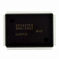
DF2437FV Renesas Electronics America, DF2437FV Datasheet - Page 616

DF2437FV
Manufacturer Part Number
DF2437FV
Description
IC H8S/2437 MCU FLASH 128QFP
Manufacturer
Renesas Electronics America
Series
H8® H8S/2400r
Specifications of DF2437FV
Core Processor
H8S/2600
Core Size
16-Bit
Speed
20MHz
Connectivity
I²C, SCI
Peripherals
POR, PWM, WDT
Number Of I /o
85
Program Memory Size
256KB (256K x 8)
Program Memory Type
FLASH
Ram Size
16K x 8
Voltage - Supply (vcc/vdd)
3 V ~ 3.6 V
Data Converters
A/D 16x10b
Oscillator Type
Internal
Operating Temperature
-20°C ~ 75°C
Package / Case
128-QFP
Lead Free Status / RoHS Status
Lead free / RoHS Compliant
Eeprom Size
-
Available stocks
Company
Part Number
Manufacturer
Quantity
Price
Company:
Part Number:
DF2437FV
Manufacturer:
Renesas Electronics America
Quantity:
10 000
- Current page: 616 of 776
- Download datasheet (5Mb)
The system configuration diagram in boot mode is shown in figure 20.6. For details on the pin
setting in boot mode, see table 20.5. The NMI and other interrupts are ignored in boot mode.
However, the NMI and other interrupts should be disabled in the system.
(1) SCI Interface Setting by Host
When boot mode is initiated, this LSI measures the low period of asynchronous SCI-communica-
tion data (H'00), which is transmitted consecutively by the host. The SCI transmit/receive format
should be set to 8-bit data, 1 stop bit, and no parity. This LSI calculates the bit rate which is
transmitted by the host according to the measured low period and transmits the bit adjustment end
sign (1 byte of H'00) to the host. The host must confirm that this bit adjustment end sign (H'00)
has been received normally and transmit 1 byte of H'55 to this LSI. When reception is not
performed normally, boot mode is initiated again (reset) and the operation described above must
be executed. The bit rates of the host and this LSI do not match according to the bit rate
transmitted by the host and system clock frequency of this LSI. To operate the SCI normally, the
transfer bit rate of the host must be set to 4,800 bps, 9,600 bps, or 19,200 bps.
The system clock frequency, which can automatically adjust the transfer bit rate of the host and
the bit rate of this LSI, is shown in table 20.6. Boot mode must be initiated in the range of this
system clock.
Rev.2.00 May. 28, 2009 Page 576 of 732
REJ09B0059-0200
tool and program
Figure 20.7 Automatic-Bit-Rate Adjustment Operation of SCI
programming
Boot
Host
data
Start
bit
Figure 20.6 System Configuration in Boot Mode
D0
Measure low period (9 bits) (data is H'00)
Control command, program data
D1
Reply response
D2
D3
D4
analysis execution
Control command,
software (on-chip)
RxD1
TxD1
On-chip SCI_1
D5
D6
This LSI
D7
On-chip RAM
High period of
at least 1 bit
Stop bit
memory
Flash
Related parts for DF2437FV
Image
Part Number
Description
Manufacturer
Datasheet
Request
R

Part Number:
Description:
KIT STARTER FOR M16C/29
Manufacturer:
Renesas Electronics America
Datasheet:

Part Number:
Description:
KIT STARTER FOR R8C/2D
Manufacturer:
Renesas Electronics America
Datasheet:

Part Number:
Description:
R0K33062P STARTER KIT
Manufacturer:
Renesas Electronics America
Datasheet:

Part Number:
Description:
KIT STARTER FOR R8C/23 E8A
Manufacturer:
Renesas Electronics America
Datasheet:

Part Number:
Description:
KIT STARTER FOR R8C/25
Manufacturer:
Renesas Electronics America
Datasheet:

Part Number:
Description:
KIT STARTER H8S2456 SHARPE DSPLY
Manufacturer:
Renesas Electronics America
Datasheet:

Part Number:
Description:
KIT STARTER FOR R8C38C
Manufacturer:
Renesas Electronics America
Datasheet:

Part Number:
Description:
KIT STARTER FOR R8C35C
Manufacturer:
Renesas Electronics America
Datasheet:

Part Number:
Description:
KIT STARTER FOR R8CL3AC+LCD APPS
Manufacturer:
Renesas Electronics America
Datasheet:

Part Number:
Description:
KIT STARTER FOR RX610
Manufacturer:
Renesas Electronics America
Datasheet:

Part Number:
Description:
KIT STARTER FOR R32C/118
Manufacturer:
Renesas Electronics America
Datasheet:

Part Number:
Description:
KIT DEV RSK-R8C/26-29
Manufacturer:
Renesas Electronics America
Datasheet:

Part Number:
Description:
KIT STARTER FOR SH7124
Manufacturer:
Renesas Electronics America
Datasheet:

Part Number:
Description:
KIT STARTER FOR H8SX/1622
Manufacturer:
Renesas Electronics America
Datasheet:

Part Number:
Description:
KIT DEV FOR SH7203
Manufacturer:
Renesas Electronics America
Datasheet:


