DF2437FV Renesas Electronics America, DF2437FV Datasheet - Page 207
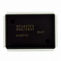
DF2437FV
Manufacturer Part Number
DF2437FV
Description
IC H8S/2437 MCU FLASH 128QFP
Manufacturer
Renesas Electronics America
Series
H8® H8S/2400r
Specifications of DF2437FV
Core Processor
H8S/2600
Core Size
16-Bit
Speed
20MHz
Connectivity
I²C, SCI
Peripherals
POR, PWM, WDT
Number Of I /o
85
Program Memory Size
256KB (256K x 8)
Program Memory Type
FLASH
Ram Size
16K x 8
Voltage - Supply (vcc/vdd)
3 V ~ 3.6 V
Data Converters
A/D 16x10b
Oscillator Type
Internal
Operating Temperature
-20°C ~ 75°C
Package / Case
128-QFP
Lead Free Status / RoHS Status
Lead free / RoHS Compliant
Eeprom Size
-
Available stocks
Company
Part Number
Manufacturer
Quantity
Price
Company:

Part Number:
DF2437FV
Manufacturer:
Renesas Electronics America
Quantity:
10 000


7.5.4
When the corresponding bit in PTCNT1 is cleared to 0, port 4 pins can be used as interrupt input
pins (IRQ7 to IRQ0). When the corresponding bit in PTCNT0 is set to 1, port 4 pins can be used
as PWM output pins (ExPW3 to ExPW0). The relationship between register setting values and pin
functions is as follows.
• P47/IRQ7/TMIY_0/ExPW3
Note:
• P46/IRQ6/TMIX_0/ExPW2
P47DDR
PW3S
OE3
Pin function
When the IRQ7S bit in PTCNT1 is cleared to 0, this pin can be used as an IRQ7 pin.
When the PW3S bit in PTCNT0 is set to 1, this pin can be used as an ExPW3 pin.
The pin function is switched as shown below according to the combination of the OE3 bit in
PWOER of the PWM, the IRQ7S bit, the PW3S bit, and the P47DDR bit.
When the external clock is selected by the CKS2 to CKS0 bits in TCR of the TMRY_0, this
pin functions as a TMCIY input pin. When the CCLR1 and CCLR0 bits in TCR of the
TMRY_0 are both set to 1, this pin functions as a TMRIY input pin.
When the IRQ6S bit in PTCNT1 is cleared to 0, this pin can be used as an IRQ6 pin.
When the PW2S bit in PTCNT0 is set to 1, this pin can be used as an ExPW2 pin.
The pin function is switched as shown below according to the combination of the OE2 bit in
PWOER of the PWM, the IRQ6S bit, the PW2S bit, and the P46DDR bit.
When the external clock is selected by the CKS2 to CKS0 bits in TCR of the TMRX_0, this
pin functions as a TMCIX input pin. When the CCLR1 and CCLR0 bits in TCR of the
TMRX_0 are both set to 1, this pin functions as a TMRIX input pin.
* When the IRQ7S bit in PTCNT1 is cleared to 0, this pin functions as the IRQ7 input pin.
Pin Functions
P47 input pin
⎯
⎯
0
P47 output pin
TMIY_0 (TMCIY/TMRIY) input pin
⎯
0
IRQ7 input pin*
P47 output pin
Rev.2.00 May. 28, 2009 Page 167 of 732
0
1
1
PW3 output pin
REJ09B0059-0200
1
Related parts for DF2437FV
Image
Part Number
Description
Manufacturer
Datasheet
Request
R

Part Number:
Description:
KIT STARTER FOR M16C/29
Manufacturer:
Renesas Electronics America
Datasheet:

Part Number:
Description:
KIT STARTER FOR R8C/2D
Manufacturer:
Renesas Electronics America
Datasheet:

Part Number:
Description:
R0K33062P STARTER KIT
Manufacturer:
Renesas Electronics America
Datasheet:

Part Number:
Description:
KIT STARTER FOR R8C/23 E8A
Manufacturer:
Renesas Electronics America
Datasheet:

Part Number:
Description:
KIT STARTER FOR R8C/25
Manufacturer:
Renesas Electronics America
Datasheet:

Part Number:
Description:
KIT STARTER H8S2456 SHARPE DSPLY
Manufacturer:
Renesas Electronics America
Datasheet:

Part Number:
Description:
KIT STARTER FOR R8C38C
Manufacturer:
Renesas Electronics America
Datasheet:

Part Number:
Description:
KIT STARTER FOR R8C35C
Manufacturer:
Renesas Electronics America
Datasheet:

Part Number:
Description:
KIT STARTER FOR R8CL3AC+LCD APPS
Manufacturer:
Renesas Electronics America
Datasheet:
Part Number:
Description:
KIT STARTER FOR RX610
Manufacturer:
Renesas Electronics America
Datasheet:

Part Number:
Description:
KIT STARTER FOR R32C/118
Manufacturer:
Renesas Electronics America
Datasheet:

Part Number:
Description:
KIT DEV RSK-R8C/26-29
Manufacturer:
Renesas Electronics America
Datasheet:

Part Number:
Description:
KIT STARTER FOR SH7124
Manufacturer:
Renesas Electronics America
Datasheet:

Part Number:
Description:
KIT STARTER FOR H8SX/1622
Manufacturer:
Renesas Electronics America
Datasheet:

Part Number:
Description:
KIT DEV FOR SH7203
Manufacturer:
Renesas Electronics America
Datasheet: