DF2437FV Renesas Electronics America, DF2437FV Datasheet - Page 16
DF2437FV
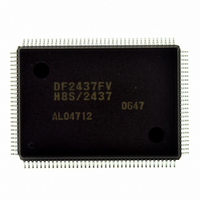
Manufacturer Part Number
DF2437FV
Description
IC H8S/2437 MCU FLASH 128QFP
Manufacturer
Renesas Electronics America
Series
H8® H8S/2400r
Specifications of DF2437FV
Core Processor
H8S/2600
Core Size
16-Bit
Speed
20MHz
Connectivity
I²C, SCI
Peripherals
POR, PWM, WDT
Number Of I /o
85
Program Memory Size
256KB (256K x 8)
Program Memory Type
FLASH
Ram Size
16K x 8
Voltage - Supply (vcc/vdd)
3 V ~ 3.6 V
Data Converters
A/D 16x10b
Oscillator Type
Internal
Operating Temperature
-20°C ~ 75°C
Package / Case
128-QFP
Lead Free Status / RoHS Status
Lead free / RoHS Compliant
Eeprom Size
-
Available stocks
Company
Part Number
Manufacturer
Quantity
Price
Company:

Part Number:
DF2437FV
Manufacturer:
Renesas Electronics America
Quantity:
10 000


9.4
9.5
Section 10 16-Bit Free-Running Timer (FRT)..................................................247
10.1 Features............................................................................................................................. 247
10.2 Input/Output Pins .............................................................................................................. 249
10.3 Register Descriptions ........................................................................................................ 249
10.4 Operation .......................................................................................................................... 259
10.5 Operation Timing.............................................................................................................. 260
10.6 Interrupt Sources............................................................................................................... 268
10.7 Usage Notes ...................................................................................................................... 269
Section 11 8-Bit Timer (TMR)..........................................................................275
11.1 Features............................................................................................................................. 275
Rev.2.00 May. 28, 2009 Page xiv of xxxviii
REJ09B0059-0200
9.3.1
9.3.2
9.3.3
9.3.4
Bus Master Interface ......................................................................................................... 240
Operation .......................................................................................................................... 241
10.3.1 Free-Running Counter (FRC) .............................................................................. 250
10.3.2 Output Compare Registers A and B (OCRA and OCRB) ................................... 250
10.3.3 Input Capture Registers A to D (ICRA to ICRD) ................................................ 250
10.3.4 Output Compare Registers AR and AF (OCRAR and OCRAF) ......................... 251
10.3.5 Output Compare Register DM (OCRDM) ........................................................... 251
10.3.6 Timer Interrupt Enable Register (TIER) .............................................................. 252
10.3.7 Timer Control/Status Register (TCSR)................................................................ 253
10.3.8 Timer Control Register (TCR)............................................................................. 256
10.3.9 Timer Output Compare Control Register (TOCR) .............................................. 257
10.4.1 Pulse Output......................................................................................................... 259
10.5.1 FRC Increment Timing ........................................................................................ 260
10.5.2 Output Compare Output Timing .......................................................................... 261
10.5.3 FRC Clear Timing ............................................................................................... 261
10.5.4 Input Capture Input Timing ................................................................................. 262
10.5.5 Buffered Input Capture Input Timing .................................................................. 263
10.5.6 Timing of Input Capture Flag Setting .................................................................. 264
10.5.7 Timing of Output Compare Flag Setting ............................................................. 265
10.5.8 Timing of Overflow Flag Setting......................................................................... 266
10.5.9 Automatic Addition Timing................................................................................. 266
10.5.10 Mask Signal Generation Timing .......................................................................... 267
10.7.1 Conflict between FRC Write and Clear ............................................................... 269
10.7.2 Conflict between FRC Write and Increment........................................................ 270
10.7.3 Conflict between OCR Write and Compare-Match ............................................. 271
10.7.4 Switching of Internal Clock and FRC Operation ................................................. 272
PWMX (D/A) Counters H and L (DACNTH and DACNTL) ............................. 235
PWMX (D/A) Data Registers A and B (DADRA and DADRB)......................... 236
PWMX (D/A) Control Register (DACR) ............................................................ 238
Peripheral Clock Select Register (PCSR) ............................................................ 239
Related parts for DF2437FV
Image
Part Number
Description
Manufacturer
Datasheet
Request
R

Part Number:
Description:
KIT STARTER FOR M16C/29
Manufacturer:
Renesas Electronics America
Datasheet:

Part Number:
Description:
KIT STARTER FOR R8C/2D
Manufacturer:
Renesas Electronics America
Datasheet:

Part Number:
Description:
R0K33062P STARTER KIT
Manufacturer:
Renesas Electronics America
Datasheet:

Part Number:
Description:
KIT STARTER FOR R8C/23 E8A
Manufacturer:
Renesas Electronics America
Datasheet:

Part Number:
Description:
KIT STARTER FOR R8C/25
Manufacturer:
Renesas Electronics America
Datasheet:

Part Number:
Description:
KIT STARTER H8S2456 SHARPE DSPLY
Manufacturer:
Renesas Electronics America
Datasheet:

Part Number:
Description:
KIT STARTER FOR R8C38C
Manufacturer:
Renesas Electronics America
Datasheet:

Part Number:
Description:
KIT STARTER FOR R8C35C
Manufacturer:
Renesas Electronics America
Datasheet:

Part Number:
Description:
KIT STARTER FOR R8CL3AC+LCD APPS
Manufacturer:
Renesas Electronics America
Datasheet:
Part Number:
Description:
KIT STARTER FOR RX610
Manufacturer:
Renesas Electronics America
Datasheet:

Part Number:
Description:
KIT STARTER FOR R32C/118
Manufacturer:
Renesas Electronics America
Datasheet:

Part Number:
Description:
KIT DEV RSK-R8C/26-29
Manufacturer:
Renesas Electronics America
Datasheet:

Part Number:
Description:
KIT STARTER FOR SH7124
Manufacturer:
Renesas Electronics America
Datasheet:

Part Number:
Description:
KIT STARTER FOR H8SX/1622
Manufacturer:
Renesas Electronics America
Datasheet:

Part Number:
Description:
KIT DEV FOR SH7203
Manufacturer:
Renesas Electronics America
Datasheet: