DF2437FV Renesas Electronics America, DF2437FV Datasheet - Page 133
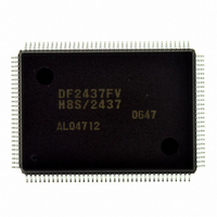
DF2437FV
Manufacturer Part Number
DF2437FV
Description
IC H8S/2437 MCU FLASH 128QFP
Manufacturer
Renesas Electronics America
Series
H8® H8S/2400r
Specifications of DF2437FV
Core Processor
H8S/2600
Core Size
16-Bit
Speed
20MHz
Connectivity
I²C, SCI
Peripherals
POR, PWM, WDT
Number Of I /o
85
Program Memory Size
256KB (256K x 8)
Program Memory Type
FLASH
Ram Size
16K x 8
Voltage - Supply (vcc/vdd)
3 V ~ 3.6 V
Data Converters
A/D 16x10b
Oscillator Type
Internal
Operating Temperature
-20°C ~ 75°C
Package / Case
128-QFP
Lead Free Status / RoHS Status
Lead free / RoHS Compliant
Eeprom Size
-
Available stocks
Company
Part Number
Manufacturer
Quantity
Price
Company:

Part Number:
DF2437FV
Manufacturer:
Renesas Electronics America
Quantity:
10 000


This LSI has an on-chip bus controller (BSC) that manages the bus width and the number of
access states of the external address space.
6.1
• Extended modes
• Extended area division
• Area select signal, address strobe/hold signal polarity control
• It is possible to reverse the output polarity of CS1 to CS3 and AS/AH by the PNCCS bit in
Normal Extension:
Address output pins (A15 to A0) and data input/output pins (D15 to D0) are separate
• Usable areas
• Normal extended bus interface
• Idle cycle insertion
BSCS200A_000020020300
Two modes for external extension
Normal extended mode: Normal extension (when the ADMXE bit in BCR is 0)
Address-data multiplex extended mode: Multiplex extension (when the ADMXE bit in BCR is
1)
The external address space is divided into a basic area, and three 64-kbyte areas
The basic area and area 1 are for common settings. Area 2 and 3 bus specifications can be set
independently
Areas 1, 2, and 3 enable chip-select (CS1 to CS3) output
A maximum of 16 addresses can be output
BCRAn or the PNCASH bit in BCR
Basic area and areas 1, 2, and 3 are all usable
Selection between 2-state access area and 3-state access area is possible
Program wait state insert is possible
Idle cycle insert is possible during the external write cycle, directly after external read cycle.
Features
Section 6 Bus Controller (BSC)
Rev.2.00 May. 28, 2009 Page 93 of 732
REJ09B0059-0200
Related parts for DF2437FV
Image
Part Number
Description
Manufacturer
Datasheet
Request
R

Part Number:
Description:
KIT STARTER FOR M16C/29
Manufacturer:
Renesas Electronics America
Datasheet:

Part Number:
Description:
KIT STARTER FOR R8C/2D
Manufacturer:
Renesas Electronics America
Datasheet:

Part Number:
Description:
R0K33062P STARTER KIT
Manufacturer:
Renesas Electronics America
Datasheet:

Part Number:
Description:
KIT STARTER FOR R8C/23 E8A
Manufacturer:
Renesas Electronics America
Datasheet:

Part Number:
Description:
KIT STARTER FOR R8C/25
Manufacturer:
Renesas Electronics America
Datasheet:

Part Number:
Description:
KIT STARTER H8S2456 SHARPE DSPLY
Manufacturer:
Renesas Electronics America
Datasheet:

Part Number:
Description:
KIT STARTER FOR R8C38C
Manufacturer:
Renesas Electronics America
Datasheet:

Part Number:
Description:
KIT STARTER FOR R8C35C
Manufacturer:
Renesas Electronics America
Datasheet:

Part Number:
Description:
KIT STARTER FOR R8CL3AC+LCD APPS
Manufacturer:
Renesas Electronics America
Datasheet:
Part Number:
Description:
KIT STARTER FOR RX610
Manufacturer:
Renesas Electronics America
Datasheet:

Part Number:
Description:
KIT STARTER FOR R32C/118
Manufacturer:
Renesas Electronics America
Datasheet:

Part Number:
Description:
KIT DEV RSK-R8C/26-29
Manufacturer:
Renesas Electronics America
Datasheet:

Part Number:
Description:
KIT STARTER FOR SH7124
Manufacturer:
Renesas Electronics America
Datasheet:

Part Number:
Description:
KIT STARTER FOR H8SX/1622
Manufacturer:
Renesas Electronics America
Datasheet:

Part Number:
Description:
KIT DEV FOR SH7203
Manufacturer:
Renesas Electronics America
Datasheet: